74VCX16821
74VCX16821 is Low Voltage 20-Bit D-Type Flip-Flops manufactured by Fairchild Semiconductor.
..
74VCX16821 Low Voltage 20-Bit D-Type Flip-Flops with 3.6V Tolerant Inputs and Outputs
March 1998 Revised October 2004
74VCX16821 Low Voltage 20-Bit D-Type Flip-Flops with 3.6V Tolerant Inputs and Outputs
General Description
The VCX16821 contains twenty non-inverting D-type flipflops with 3-STATE outputs and is intended for bus oriented applications. The 74VCX16821 is designed for low voltage (1.4V to 3.6V) VCC applications with I/O patibility up to 3.6V. The 74VCX16821 is fabricated with an advanced CMOS technology to achieve high speed operation while maintaining low CMOS power dissipation.
Features s 1.4V to 3.6V VCC supply operation s 3.6V tolerant inputs and outputs s t PD 3.5 ns max for 3.0V to 3.6V VCC s Power-off high impedance inputs and outputs s Supports live insertion and withdrawal (Note 1) s Static Drive (IOH/IOL)
±24 m A @ 3.0V VCC s Uses patented noise/EMI reduction circuitry s Latch-up performance exceeds 300 m A s ESD performance: Human body model > 2000V Machine model > 200V
Note 1: To ensure the high-impedance state during power up or power down, OE should be tied to VCC through a pull-up resistor; the minimum value of the resistor is determined by the current-sourcing capability of the driver.
Ordering Code:
Order Number 74VCX16821MTD Package Number MTD56 Package Descriptions 56-Lead Thin Shrink Small Outline Package (TSSOP), JEDEC MO-153, 6.1mm Wide
Device also available in Tape and Reel. Specify by appending suffix letter “X” to the ordering code.
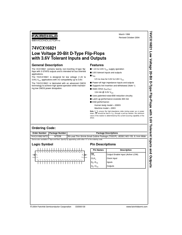
Logic Symbol
Pin Descriptions
Pin Names OEn CLKn D0- D19 O0- O19 Description Output Enable Input (Active LOW) Clock Input Inputs Outputs
© 2004 Fairchild Semiconductor Corporation
DS500130
.fairchildsemi.
Connection Diagram
Truth Tables
Inputs CLK1 OE1 H L L L Inputs CLK2 OE2 H L L L D10- D19 X L H X D0- D9 X L H X Outputs O0- O9 Z L H O0 Outputs O10- O19 Z L H O0
L or H
L or H
H = HIGH Voltage Level L = LOW Voltage Level X = Immaterial...