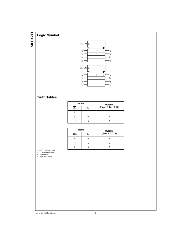
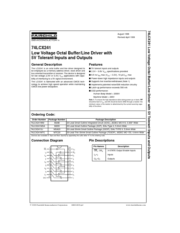
Datasheet4U Logo Datasheet4U.com

74LCX241 - Low Voltage Octal Buffer/Line Driver

Description

The LCX241 is an octal buffer and line driver designed to be employed as a memory address driver, clock driver and bus oriented transmitter or receiver.

The device is designed for low voltage (2.5V or 3.3V) VCC applications with capability of interfacing to a 5V signal environment.

Features

  • s 5V tolerant inputs and outputs s 2.3V.
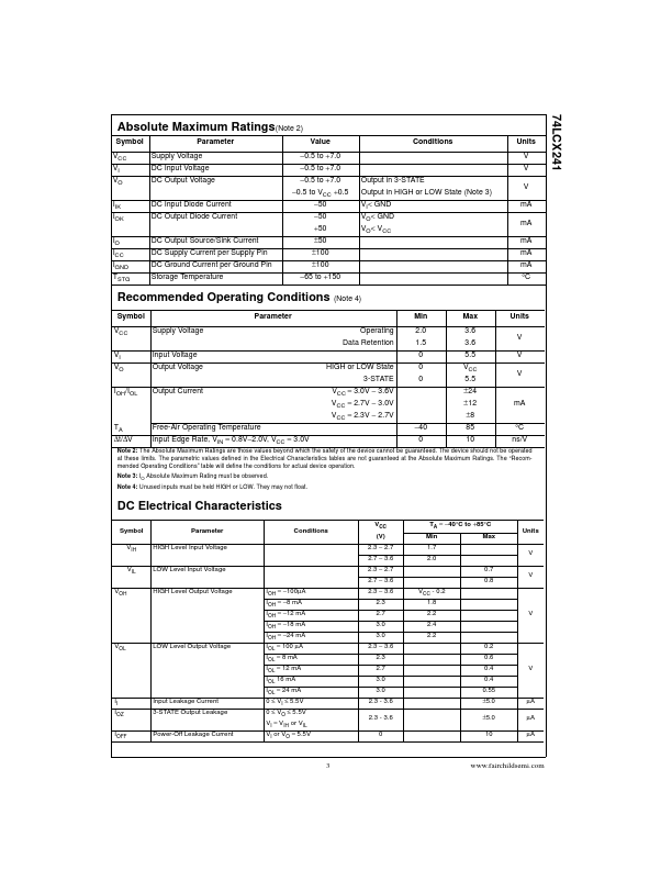
  • 3.6V VCC specifications provided s 6.5 ns tPD max (VCC = 3.3V), 10 µA ICC max s Power-down high impedance inputs and outputs s Supports live insertion/withdrawal (Note 1) s Implements patented noise/EMI reduction circuitry s Latch-up performance exceeds 500 mA s ESD performance: Human Body Model > 2000V Machine Model > 200V Note 1: To ensure the high-impedance state during power up or down, OE should be tied to VCC and OE should be tied to GND th.

📥 Download Datasheet

Full PDF Text Transcription (Reference)

The following content is an automatically extracted verbatim text from the original manufacturer datasheet and is provided for reference purposes only.

View original datasheet text
74LCX241 Low Voltage Octal Buffer/Line Driver with 5V Tolerant Inputs and Outputs August 1998 Revised April 1999 74LCX241 Low Voltage Octal Buffer/Line Driver with 5V Tolerant Inputs and Outputs General Description The LCX241 is an octal buffer and line driver designed to be employed as a memory address driver, clock driver and bus oriented transmitter or receiver. The device is designed for low voltage (2.5V or 3.3V) VCC applications with capability of interfacing to a 5V signal environment. The LCX241 is fabricated with an advanced CMOS technology to achieve high speed operation while maintaining CMOS low power dissipation. Features s 5V tolerant inputs and outputs s 2.3V – 3.6V VCC specifications provided s 6.5 ns tPD max (VCC = 3.