74ABT241 Overview
Key Specifications
Package: TSSOP
Mount Type: Surface Mount
Pins: 20
Operating Voltage: 5 V
Description
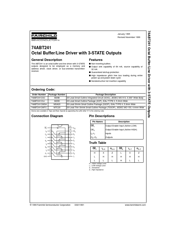
The ABT241 is an octal buffer and line driver with 3-STATE outputs designed to be employed as a memory and address driver, clock driver, or bus-oriented transmitter/ receiver.
Key Features
- H L OE2 L H H I4–7 X H L O4–7