Download NDH8502P Datasheet PDF
Fairchild Semiconductor
NDH8502P
NDH8502P is Dual P-Channel MOSFET manufactured by Fairchild Semiconductor.
Description Super SOTTM-8 P-Channel enhancement mode power field effect transistors are produced using Fairchild's proprietary, high cell density, DMOS technology. This very high density process is especially tailored to minimize on-state resistance. These devices are particularly suited for low voltage applications such as notebook puter power management and other battery powered circuits where fast high-side switching, and low in-line power loss are needed in a very small outline surface mount package. Features -2.
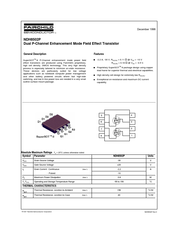
2 A, -30 V. RDS(ON) = 0.11 Ω @ VGS = -10 V RDS(ON) = 0.18 Ω @ VGS = -4.5 V. Proprietary Super SOTTM-8 package design using copper lead frame for superior thermal and electrical capabilities. High density cell design for extremely low RDS(ON). Exceptional on-resistance and maximum DC current capability. 4 3 2 7 8 Absolute Maximum Ratings T A = 25°C unless otherwise noted Symbol VDSS VGSS ID PD TJ,TSTG Parameter Drain-Source Voltage Gate-Source Voltage Drain Current - Continuous - Pulsed Maximum Power Dissipation Operating and Storage Temperature Range (Note 1) (Note 1) NDH8502P -30 ±20 -2.2 -10 0.8 -55 to 150 Units V V A W °C THERMAL CHARACTERISTICS RθJA RθJC Thermal Resistance, Junction-to-Ambient Thermal Resistance, Junction-to-Case (Note 1) (Note 1) 156 40 °C/W °C/W © 1997 Fairchild Semiconductor Corporation NDH8502P Rev.C ELECTRICAL CHARACTERISTICS (TA = 25°C unless otherwise noted) Symbol Parameter Conditions Min Typ Max Units OFF CHARACTERISTICS BVDSS IDSS IGSSF IGSSR VGS(th) RDS(ON) Drain-Source Breakdown Voltage Zero Gate Voltage Drain Current VGS = 0 V, ID = -250 µA VDS = -24 V, VGS = 0 V TJ= 55°C Gate - Body Leakage, Forward Gate - Body Leakage, Reverse VGS = 20 V, VDS = 0 V VGS = -20 V, VDS= 0 V VDS = VGS, ID = - 250 µA TJ= 125°C Static Drain-Source On-Resistance VGS = -10 V, ID = -2.2 A TJ= 125°C VGS = -4.5 V, ID = -1.7 A ID(on) g FS...