NDB7050L
NDB7050L is N-Channel MOSFET manufactured by Fairchild Semiconductor.
Description
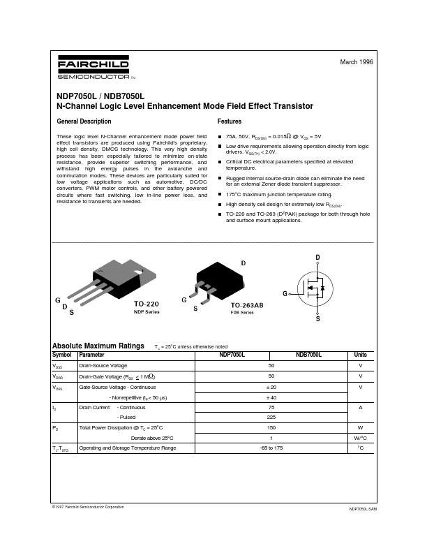
These logic level N-Channel enhancement mode power field effect transistors are produced using Fairchild's proprietary, high cell density, DMOS technology. This very high density process has been especially tailored to minimize on-state resistance, provide superior switching performance, and withstand high energy pulses in the avalanche and mutation modes. These devices are particularly suited for low voltage applications such as automotive, DC/DC converters, PWM motor controls, and other battery powered circuits where fast switching, low in-line power loss, and resistance to transients are needed.
Features
75A, 50V, RDS(ON) = 0.015Ω @ VGS = 5V Low drive requirements allowing operation directly from logic drivers. VGS(TH) < 2.0V. Critical DC electrical parameters specified at elevated temperature. Rugged internal source-drain diode can eliminate the need for an external Zener diode transient suppressor. 175°C maximum junction temperature rating. High density cell design for extremely low RDS(ON). TO-220 and TO-263 (D2PAK) package for both through hole and surface mount applications.
Absolute Maximum Ratings
Symbol VDSS VDGR VGSS ID Parameter Drain-Source Voltage
T C = 25°C unless otherwise noted
NDP7050L 50 50 ± 20 ± 40 75 225 150 1 -65 to 175
Units V V V
Drain-Gate Voltage (RGS < 1 MΩ) Gate-Source Voltage
- Continuous
- Nonrepetitive (t P < 50 µs) Drain Current
- Continuous
- Pulsed
Total Power Dissipation @ TC = 25°C Derate above 25°C
W W/°C °C
TJ,TSTG
Operating and Storage Temperature Range
© 1997 Fairchild Semiconductor Corporation
NDP7050L.SAM
Electrical Characteristics (TC = 25°C unless otherwise noted)
Symbol Parameter Conditions Min Typ Max Units DRAIN-SOURCE AVALANCHE RATINGS (Note 1) W DSS IAR BVDSS IDSS IGSSF IGSSR VGS(th) RDS(ON) ID(on) g FS Single Pulse Drain-Source Avalanche Energy Maximum Drain-Source Avalanche Current VDD...