IRFS830B
IRFS830B is 500V N-Channel MOSFET manufactured by Fairchild Semiconductor.
Description
These N-Channel enhancement mode power field effect transistors are produced using Fairchild’s proprietary, planar, DMOS technology. This advanced technology has been especially tailored to minimize on-state resistance, provide superior switching performance, and withstand high energy pulse in the avalanche and mutation mode. These devices are well suited for high efficiency switch mode power supplies, power factor correction and electronic lamp ballasts based on half bridge.
Features
- -
- -
- - 4.5A, 500V, RDS(on) = 1.5Ω @VGS = 10 V Low gate charge ( typical 27 n C) Low Crss ( typical 17 p F) Fast switching 100% avalanche tested Improved dv/dt capability
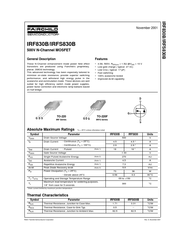
G G DS
TO-220
IRF Series
GD S
TO-220F
IRFS Series
Absolute Maximum Ratings
Symbol VDSS ID IDM VGSS EAS IAR EAR dv/dt PD TJ, TSTG TL
TC = 25°C unless otherwise noted
Parameter Drain-Source Voltage
- Continuous (TC = 25°C) Drain Current
- Continuous (TC = 100°C) Drain Current
- Pulsed
(Note 1)
IRF830B 500 4.5 2.9 18 ± 30
(Note 2) (Note 1) (Note 1) (Note 3)
IRFS830 4.5
- 2.9
- 18
- 270 4.5 7.3 5.5
Units V A A A V m J A m J V/ns W W/°C °C °C
Gate-Source Voltage Single Pulsed Avalanche Energy Avalanche Current Repetitive Avalanche Energy Peak Diode Recovery dv/dt Power Dissipation (TC = 25°C)
- Derate above 25°C Operating and Storage Temperature Range Maximum lead temperature for soldering purposes, 1/8" from case for 5 seconds
73 0.58 -55 to +150 300
38 0.3
- Drain current limited by maximum junction temperature
Thermal Characteristics
Symbol RθJC RθCS RθJA Parameter Thermal Resistance, Junction-to-Case Max. Thermal Resistance, Case-to-Sink Typ. Thermal Resistance, Junction-to-Ambient Max. IRF830B 1.71 0.5 62.5 IRFS830B 3.31 -62.5 Units °C/W °C/W °C/W
©2001 Fairchild Semiconductor Corporation
Rev. A, November 2001
IRF830B/IRFS830B
Electrical Characteristics...