The following content is an automatically extracted verbatim text
from the original manufacturer datasheet and is provided for reference purposes only.
View original datasheet text
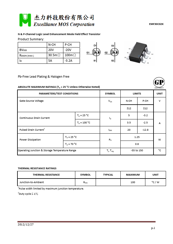
N & P‐Channel Logic Level Enhancement Mode Field Effect Transistor
Product Summary:
N‐CH
P‐CH
BVDSS
20V
‐20V
RDSON (MAX.)
30.5mΩ 100mΩ
ID
5A
‐3.2A
EMF30C02K
Pb‐Free Lead Plating & Halogen Free
ABSOLUTE MAXIMUM RATINGS (TA = 25 °C Unless Otherwise Noted) PARAMETERS/TEST CONDITIONS
SYMBOL
Gate‐Source Voltage
VGS
Continuous Drain Current Pulsed Drain Current1
TA = 25 °C TA = 100 °C
Power Dissipation
TA = 25 °C TA = 70 °C
Operating Junction & Storage Temperature Range
ID IDM PD Tj, Tstg
LIMITS
N‐CH
P‐CH
±12
±12
5
‐3.2
3.5
‐2.5
20
‐12.8
1.25
0.8 ‐55 to 150
UNIT V
A W °C
THERMAL RESISTANCE RATINGS THERMAL RESISTANCE
SYMBOL
Junction‐to‐Ambient
RJA
1Pulse width limited by maximum junction temperature.
 EMF30C02K Datasheet