The following content is an automatically extracted verbatim text
from the original manufacturer datasheet and is provided for reference purposes only.
View original datasheet text
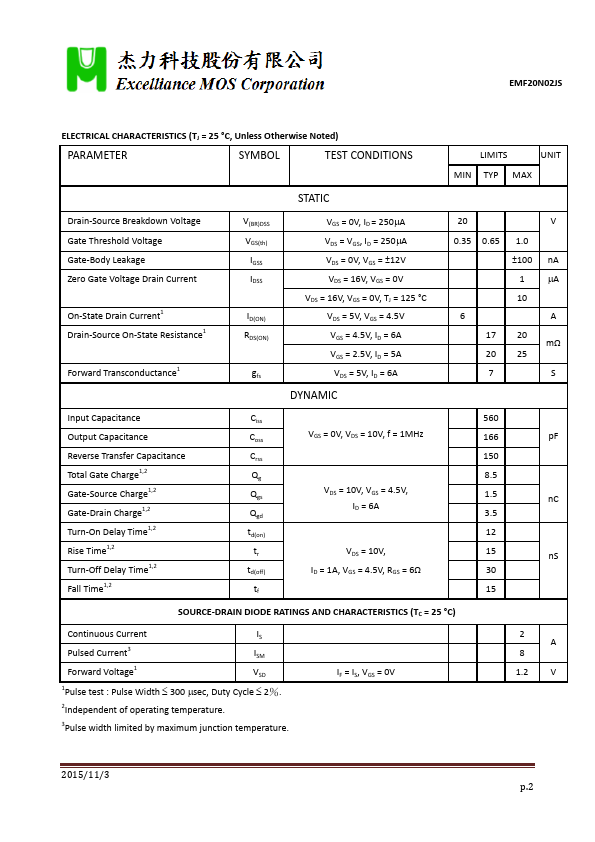
N‐Channel Logic Level Enhancement Mode Field Effect Transistor
Product Summary:
BVDSS
20V
D
RDSON (MAX.)
20mΩ
ID
6A
G
S Pb‐Free Lead Plating & Halogen Free
ABSOLUTE MAXIMUM RATINGS (TA = 25 °C Unless Otherwise Noted) PARAMETERS/TEST CONDITIONS
SYMBOL
Gate‐Source Voltage
Continuous Drain Current Pulsed Drain Current1
TA = 25 °C TA = 70 °C
Power Dissipation
TA = 25 °C TA = 70 °C
Operating Junction & Storage Temperature Range
VGS ID IDM PD Tj, Tstg
EMF20N02JS
LIMITS ±12 6 4 24 1.04 0.66
‐55 to 150
UNIT V
A
W °C
THERMAL RESISTANCE RATINGS THERMAL RESISTANCE
SYMBOL
Junction‐to‐Ambient3
RJA (T ≤ 10sec) RJA (Steady State)
1Pulse width limited by maximum junction temperature. 2Duty cycle 1% 3The device mounted on a 1 in2 pad of 2 oz copper.
 EMF20N02JS Datasheet