XRP7657
XRP7657 is 25V Non Synchronous PWM Step Down Regulator manufactured by Exar.
February 2011
2A, 25V Non Synchronous PWM Step Down Regulator
Rev. 2.0.0
GENERAL DESCRIPTION
The XRP7657 is a non synchronous voltage mode PWM step down (buck) regulator capable of a constant output current up to 2Amps. A wide 4.75V to 25V input voltage range allows for single supply operations from industry standard 5V, 12V and 24V power rails.
With a 420k Hz constant operating frequency and integrated high side switch, the XRP7657 reduces the overall ponent count and solution footprint. In addition to a 2% output setpoint accuracy, this device provides high efficiency, low ripple and excellent line and load regulation. An enable function and soft start feature allow for controlled power up sequencing implementation.
Built-in over current, output short-circuit and over temperature protection insure safe operations under abnormal operating conditions.
The XRP7657 is offered in a Ro HS pliant, “green”/halogen free 8-pin SOIC package.
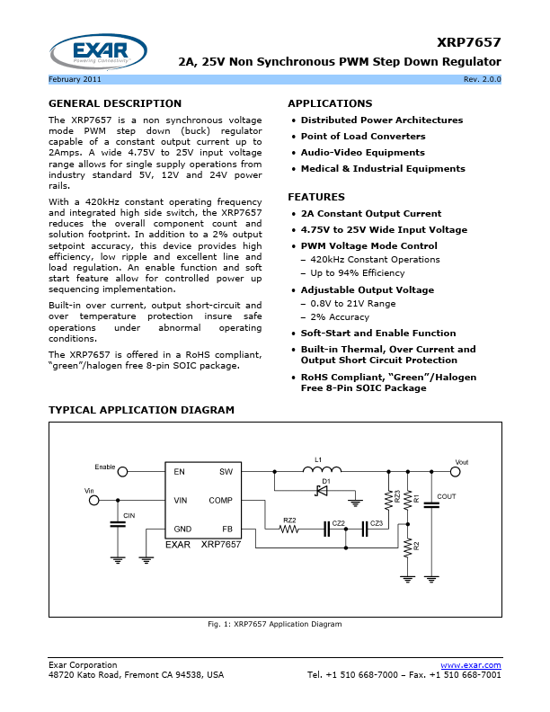
TYPICAL APPLICATION DIAGRAM
APPLICATIONS
- Distributed Power Architectures
- Point of Load Converters
- Audio-Video Equipments
- Medical & Industrial Equipments
Features
- 2A Constant Output Current
- 4.75V to 25V Wide Input Voltage
- PWM Voltage Mode Control
- 420k Hz Constant Operations
- Up to 94% Efficiency
- Adjustable Output Voltage
- 0.8V to 21V Range
- 2% Accuracy
- Soft-Start and Enable Function
- Built-in Thermal, Over Current and Output Short Circuit Protection
- Ro HS pliant, “Green”/Halogen Free 8-Pin SOIC Package
Fig. 1: XRP7657 Application Diagram
Exar Corporation 48720 Kato Road, Fremont CA 94538, USA
.exar. Tel. +1 510 668-7000
- Fax. +1 510...