Crystal oscillator
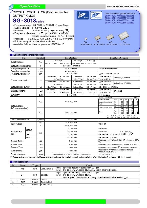
CRYSTAL OSCILLATOR (Programmable)
OUTPUT: CMOS
SG - 8018series
• Frequency range : 0.67 MHz to 170 MHz (1 ppm Step)
• Supply voltage : 1.62 V to 3.63 V
• Function
: Output enable (OE) or Standby (S¯¯T)
• Frequency tolerance : ±50 ppm (-40 ºC to +105 ºC)
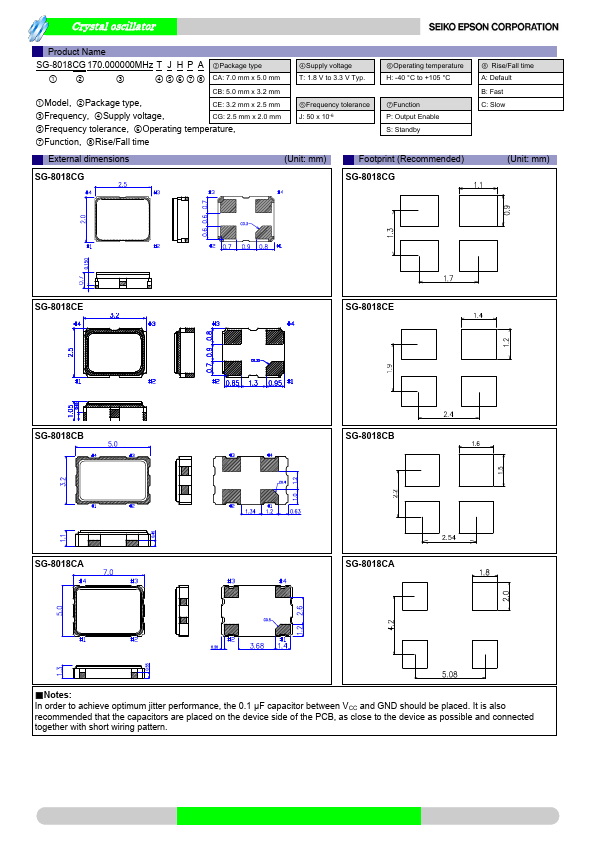
Include frequency aging(+25 ºC, 10 years)
• Package :2.5 x 2.0, 3.2 x 2.5, 5.0 x 3.2, 7.0 x 5.0 (mm)
• PLL technology to enable short lead time
• Available field oscillator programmer “SG-Writer II”
Product Number (please contact us)
SG-8018CA: X1G005571xxxx00
SG-8018CB: X1G005581xxxx00
SG-8018CE: X1G005591xxxx00
SG-8018CG: X1G005601xxxx00
CG CE CB
CA
2.5 x 2.0mm 3.2 x 2.5mm 5.0 x 3.2mm 7.0 x 5.0mm
2.5x2.0mm
Specifications (characteristics)
Item
Symbol
Specifications
Conditions/Remarks
Supply voltage
VCC
1.80 V Typ.
2.50 V Typ.
3.30 V Typ.
1.62 V to 1.98 V 1.98 V to 2.20 V 2.20 V to 2.80 V 2.70 V to 3.63 V
-
Output frequency range
Storage temperature
Operating temperature
Frequency tolerance*1
fO
T_stg
T_use
f_tol
0.67 MHz to 170 MHz
-40 ºC to +125 ºC
-40 ºC to +105 ºC
J: ±50 × 10-6
Storage as single product.
-
T_use = -40 ºC to +105 ºC
Current consumption
3.2 mA Max. 3.3 mA Max.
2.7 mA Typ.
3.4 mA Max.
2.9 mA Typ.
3.5 mA Max.
3.0 mA Typ.
T_use = +105 ºC
T_use = +25 ºC
No load, fO = 20 MHz
ICC
5.5 mA Max. 5.8 mA Max.
4.7 mA Typ.
6.7 mA Max.
5.7 mA Typ.
8.1 mA Max.
6.8 mA Typ.
T_use = +105 ºC
T_use = +25 ºC
No load, fO = 170 MHz
Output disable current
Standby current
I_dis
I_std
3.2 mA Max.
0.9 μA Max.
0.3 μA Typ.
3.2 mA Max.
1.0 μA Max.
0.4 μA Typ.
3.3 mA Max.
1.5 μA Max.
0.5 μA Typ.
3.5 mA Max.
2.5 μA Max.
1.1 μA Typ.
OE = GND, fO = 170 MHz
T_use = +105 ºC
T_use = +25 ºC
S¯¯T = GND
Symmetry
Output voltage
(DC characteristics)
Output load condition
SYM
VOH
VOL
L_CMOS
45 % to 55 %
90 % VCC Min.
10 % VCC Max.
15 pF Max.
50 % VCC Level
IOH/IOL Conditions
[mA]
Rise/Fall time
VCC *A *B *C *D
Default (fO > 40 MHz), IOH
Fast
IOL
-2.5 -3.5 -4.0 -5.0
2.5 3.5 4.0 5.0
Default (fO ≤ 40 MHz)
IOH
IOL
-1.5 -2.0 -2.5 -3.0
1.5 2.0 2.5 3.0
Slow
IOH -1.0 -1.5 -2.0 -2.5
IOL 1.0 1.5 2.0 2.5
*A: 1.62 V to 1.98 V, *B: 1.98 V to 2.20 V,
*C: 2.20 V to 2.80 V, *D: 2.70 V to 3.63 V
-
Input voltage
VIH
VIL
70 % VCC Min.
30 % VCC Max.
OE or S¯¯T
Rise and Fall
time
Default
Fast
tr/tf
3.0 ns Max.
6.0 ns Max.
3.0 ns Max.
fO > 40 MHz
fO ≤ 40 MHz
20 % - 80 % VCC,
fO = 0.67 MHz to 170 MHz L_CMOS = 15 pF
Disable Time
Enable Time
Slow
t_stp
t_sta
10.0 ns Max.
1 μs Max.
1 μs Max.
fO = 0.67 MHz to 20 MHz
Measured from the time OE or S¯¯T pin crosses 30 %
VCC
Measured from the time OE pin crosses 70 % VCC
Resume Time
Start-up time
Frequency aging
t_res
t_str
f_aging
3 ms Max.
3 ms Max.
This is included in frequency tolerance specification.
Measured from the time S¯¯T pin crosses 70 % VCC
Measured from the time VCC reaches its rated
minimum value, 1.62 V
+25 °C, 10 years
*1 Frequency tolerance includes initial frequency tolerance, temperature variation, supply voltage variation, reflow drift, load drift and aging (+25 ºC, 10 years).
Pin description
Pin Name
OE
1
S¯¯T
2 GND
3 OUT
4 VCC
I/O type
Input Output enable
Input Standby
Power
Output
Power
Ground
Clock output
Power supply
High:
Low:
High:
Low:
Function
Specified frequency output from OUT pin
Out pin is low (weak pull down), only output driver is disabled.
Specified frequency output from OUT pin
Out pin is low (weak pull down),
Device goes to standby mode. Supply current reduces to the least as I_std.