QL2009-XPQ208C
QL2009-XPQ208C is 3.3V and 5.0V pASIC 2 FPGA Combining Speed/ Density/ Low Cost and Flexibility manufactured by Unknown Manufacturer.
- Part of the QL2 comparator family.
- Part of the QL2 comparator family.
Features
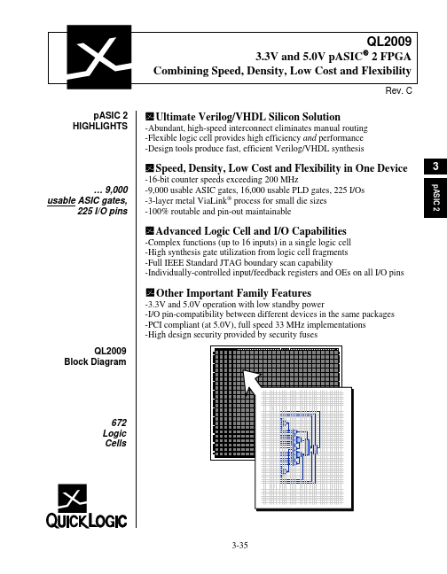
-3.3V and 5.0V operation with low standby power -I/O pin-patibility between different devices in the same packages -PCI pliant (at 5.0V), full speed 33 MHz implementations -High design security provided by security fuses QL2009 Block Diagram
672 Logic Cells
3-35
QL2009
PRODUCT SUMMARY The QL2009 is a 9,000 usable ASIC gate,16,000 usable PLD gate member of the p ASIC 2 family of FPGAs. p ASIC 2 FPGAs employ a unique bination of architecture, technology, and software tools to provide high speed, high usable density, low price, and flexibility in the same devices. The flexibility and speed make p ASIC 2 devices an efficient and high performance silicon solution for designs described using HDLs such as Verilog and VHDL, as well as schematics. The QL2009 contains 672 logic cells. With 225 maximum I/Os, the QL2009 is available in 144-pin TQFP, 208-PQFP, and 256-pin PBGA packages. Software support for the plete p ASIC families, including the QL2009, is available through three basic packages. The turnkey Quick Works® package provides the most plete FPGA software solution from design entry to logic synthesis (by Synplicity, Inc.), to place and route, to simulation. The Quick Tools TM and Quick Chip TM packages provide a solution for designers who use Cadence, Mentor, Synopsys, Viewlogic, Veribest, or other third-party tools for design entry, synthesis, or simulation. FEATURES
Total of 225 I/O Pins
- 217 bidirectional input/output pins, PCI-pliant at 5.0V in -1/-2 speed grades
- 4 high-drive input-only pins
- 4 high-drive input/distributed network pins
Four Low-Skew (less than 0.5ns) Distributed Networks
- Two array networks available to logic cell flip-flop clock, set, and reset
- each driven by an input-only pin
- Two global clock/control networks available to F1 logic input, and logic cell flip-flop clock, set, reset; input and I/O register clock, reset, enable; and output enable controls
- each driven by an input-only pin, or any input or I/O pin, or any logic cell...