M14D5121632A-1.8BG2A
M14D5121632A-1.8BG2A is DDR-II SDRAM manufactured by Elite Semiconductor Microelectronics Technology.
- Part of the M14D5121632A-1.5BG2A comparator family.
- Part of the M14D5121632A-1.5BG2A comparator family.
Features
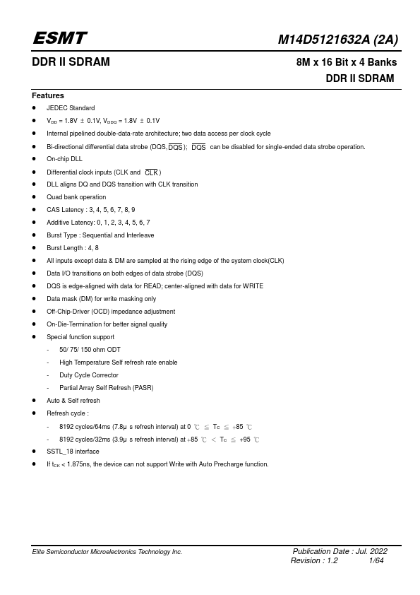
- JEDEC Standard
- VDD = 1.8V ± 0.1V, VDDQ = 1.8V ± 0.1V
- Internal pipelined double-data-rate architecture; two data access per clock cycle
- Bi-directional differential data strobe (DQS, DQS ); DQS can be disabled for single-ended data strobe operation.
- On-chip DLL
- Differential clock inputs (CLK and CLK )
- DLL aligns DQ and DQS transition with CLK transition
- Quad bank operation
- CAS Latency : 3, 4, 5, 6, 7, 8, 9
- Additive Latency: 0, 1, 2, 3, 4, 5, 6, 7
- Burst Type : Sequential and Interleave
- Burst Length : 4, 8
- All inputs except data & DM are sampled at the rising edge of the system clock(CLK)
- Data I/O transitions on both edges of data strobe (DQS)
- DQS is edge-aligned with data for READ; center-aligned with data for WRITE
- Data mask (DM) for write masking only
- Off-Chip-Driver (OCD) impedance adjustment
- On-Die-Termination for better signal quality
- Special function support
- 50/ 75/ 150 ohm ODT
- High Temperature Self refresh rate enable
- Duty Cycle Corrector
- Partial Array Self Refresh (PASR)
- Auto & Self refresh
- Refresh cycle :
- 8192 cycles/64ms (7.8μ s refresh interval) at 0 ℃ ≦ TC ≦ +85 ℃
- 8192 cycles/32ms (3.9μ s refresh interval) at +85 ℃ < TC ≦ +95 ℃
- SSTL_18 interface
- If t CK < 1.875ns, the device can not support Write with Auto Precharge function.
Elite Semiconductor Microelectronics Technology Inc.
Publication Date : Jul. 2022
Revision : 1.2
1/64
ESMT
M14D5121632A (2A)
Ordering Information:
Product ID
M14D5121632A -1.5BG2A M14D5121632A -1.8BG2A M14D5121632A -2.5BG2A M14D5121632A -1.8BBG2A M14D5121632A -2.5BBG2A
Max...


