Datasheet4U Logo Datasheet4U.com

M13S64164A-6BG - 1M x 16 Bit x 4 Banks Double Data Rate SDRAM

Download the M13S64164A-6BG datasheet PDF. This datasheet also covers the M13S64164A-5TG variant, as both devices belong to the same 1m x 16 bit x 4 banks double data rate sdram family and are provided as variant models within a single manufacturer datasheet.

Features

  • z JEDEC Standard z Internal pipelined double-data-rate architecture, two data access per clock cycle z Bi-directional data strobe (DQS) z On-chip DLL z Differential clock inputs (CLK and CLK ) z DLL aligns DQ and DQS transition with CLK transition z Quad bank operation z CAS Latency : 2, 2.5, 3 z Burst Type : Sequential and Interleave z Burst Length : 2, 4, 8 z All inputs except data & DM are sampled at the rising edge of the system clock(CLK) z Data I/O transitions on both edges of data strobe.

📥 Download Datasheet

Note: The manufacturer provides a single datasheet file (M13S64164A-5TG-ESMT.pdf) that lists specifications for multiple related part numbers.

Datasheet Details

Part number M13S64164A-6BG
Manufacturer ESMT
File Size 1.51 MB
Description 1M x 16 Bit x 4 Banks Double Data Rate SDRAM
Datasheet download datasheet M13S64164A-6BG Datasheet

Full PDF Text Transcription (Reference)

The following content is an automatically extracted verbatim text from the original manufacturer datasheet and is provided for reference purposes only.

View original datasheet text
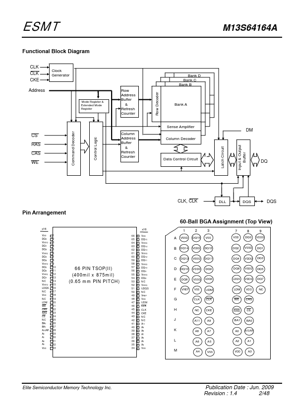
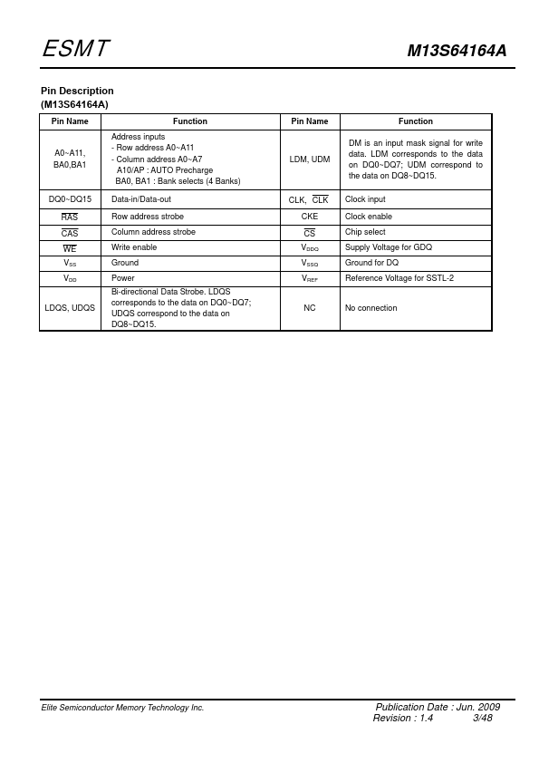
ESMT M13S64164A DDR SDRAM 1M x 16 Bit x 4 Banks Double Data Rate SDRAM Features z JEDEC Standard z Internal pipelined double-data-rate architecture, two data access per clock cycle z Bi-directional data strobe (DQS) z On-chip DLL z Differential clock inputs (CLK and CLK ) z DLL aligns DQ and DQS transition with CLK transition z Quad bank operation z CAS Latency : 2, 2.5, 3 z Burst Type : Sequential and Interleave z Burst Length : 2, 4, 8 z All inputs except data & DM are sampled at the rising edge of the system clock(CLK) z Data I/O transitions on both edges of data strobe (DQS) z DQS is edge-aligned with data for reads; center-aligned with data for WRITE z Data mask (DM) for write masking only z VDD = 2.3V ~ 2.7V, VDDQ = 2.3V ~ 2.
Published: |