Datasheet4U Logo Datasheet4U.com

F50L2G41LB-50YG2ME - 1.8V 2 Gbit (2 x 1 Gbit) SPI-NAND Flash Memory

Download the F50L2G41LB-50YG2ME datasheet PDF. This datasheet also covers the F50D2G41LB-50YG2M variant, as both devices belong to the same 1.8v 2 gbit (2 x 1 gbit) spi-nand flash memory family and are provided as variant models within a single manufacturer datasheet.

Features

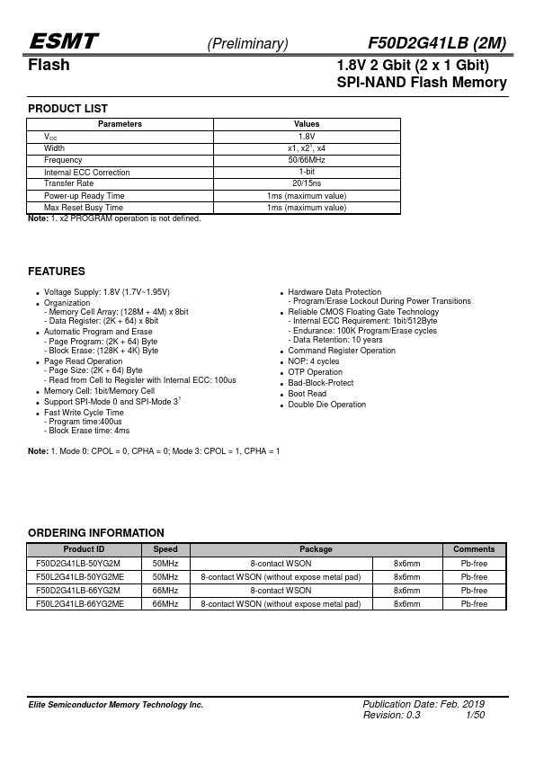
  • Voltage Supply: 1.8V (1.7V~1.95V).
  • Organization - Memory Cell Array: (128M + 4M) x 8bit - Data Register: (2K + 64) x 8bit.
  • Automatic Program and Erase - Page Program: (2K + 64) Byte - Block Erase: (128K + 4K) Byte.
  • Page Read Operation - Page Size: (2K + 64) Byte - Read from Cell to Register with Internal ECC: 100us.
  • Memory Cell: 1bit/Memory Cell.
  • Support SPI-Mode 0 and SPI-Mode 31.
  • Fast Write Cycle Time - Program time:400us - Block Erase time: 4ms.
  • Hard.

📥 Download Datasheet

Note: The manufacturer provides a single datasheet file (F50D2G41LB-50YG2M-ESMT.pdf) that lists specifications for multiple related part numbers.

Datasheet Details

Part number F50L2G41LB-50YG2ME
Manufacturer ESMT
File Size 1.25 MB
Description 1.8V 2 Gbit (2 x 1 Gbit) SPI-NAND Flash Memory
Datasheet download datasheet F50L2G41LB-50YG2ME Datasheet

Full PDF Text Transcription

Click to expand full text
ESMT Flash (Preliminary) F50D2G41LB (2M) 1.8V 2 Gbit (2 x 1 Gbit) SPI-NAND Flash Memory PRODUCT LIST Parameters VCC Width Frequency Internal ECC Correction Transfer Rate Power-up Ready Time Max Reset Busy Time Note: 1. x2 PROGRAM operation is not defined. Values 1.8V x1, x21, x4 50/66MHz 1-bit 20/15ns 1ms (maximum value) 1ms (maximum value) FEATURES  Voltage Supply: 1.8V (1.7V~1.
Published: |