Datasheet Details
| Part number | DMC1229UFDB |
|---|---|
| Manufacturer | Diodes Incorporated |
| File Size | 286.96 KB |
| Description | MOSFET |
| Datasheet |
 DMC1229UFDB Datasheet DMC1229UFDB Datasheet
|
|
|
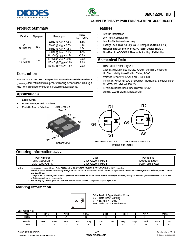
This MOSFET has been designed to minimize the on-state resistance (RDS(ON)) and yet maintain superior switching performance, making it ideal for high efficiency power management applications.
Low On-Resistance Low Input Capacitance Low Profile, 0.6mm Max Height| Part number | DMC1229UFDB |
|---|---|
| Manufacturer | Diodes Incorporated |
| File Size | 286.96 KB |
| Description | MOSFET |
| Datasheet |
DMC1229UFDB Datasheet
|
|
|
|
| Part Number | Description | Manufacturer |
|---|---|---|
| DMC16105NY-LY | LCD Module | Optrex |
| DMC16106C | 16characters x 1lines | Optrex |
| DMC16117A | LCD | Optrex |
| DMC16128NY-LY | LCD | Optrex |
| DMC16202NY-LY-ADE-BF | LCD Module | OPTREX CORPORATION |
| Part Number | Description |
|---|---|
| DMC1015UPD | MOSFET |
| DMC1016UPD | MOSFET |
| DMC1017UPD | MOSFET |
| DMC1018UPD | MOSFET |
| DMC1018UPDWQ | MOSFET |
The following content is an automatically extracted verbatim text from the original manufacturer datasheet and is provided for reference purposes only.