C147S
Key Features
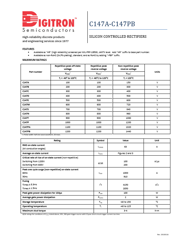
- Available as “HR” (high reliability) screened per MIL-PRF-19500, JANTX level. Add “HR” suffix to base part number
- Available as non-RoHS (Sn/Pb plating), standard, and as RoHS by adding “-PBF” suffix
| Part Number | Manufacturer | Description |
|---|---|---|
| C147S | Solid State | SILICON CONTROLLED RECTIFIERS |
| C147M | Solid State | SILICON CONTROLLED RECTIFIERS |
| C147D | Solid State | SILICON CONTROLLED RECTIFIERS |
| Q62702-C1479 | Siemens Semiconductor Group | NPN Silicon AF Transistors (For general AF applications High current gain) |
| B81133-C1474-M000 | Siemens Semiconductor Group | EMI Suppression Capacitors |
| C1473A | Panasonic | 2SC1473A |
| C1472 | Hitachi Semiconductor | 2SC1472 |
| C147PB | Solid State | SILICON CONTROLLED RECTIFIERS |
| C147T | Solid State | SILICON CONTROLLED RECTIFIERS |
| C147N | Solid State | SILICON CONTROLLED RECTIFIERS |