SLG59M1742C
SLG59M1742C is WLCSP Integrated Power Switch manufactured by Dialog Semiconductor.
An Ultra-low Power, RDSON 18 mΩ, 1 A, 0.82 mm2 WLCSP Integrated Power Switch with 550 µs Total Turn-on Time
General Description
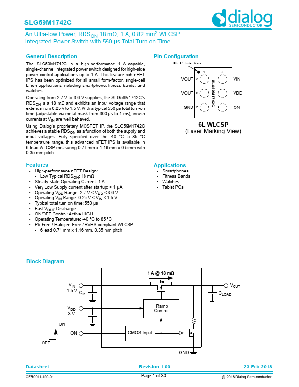
The SLG59M1742C is a high-performance 1 A capable, single-channel integrated power switch designed for high-side power control applications up to 1 A. This feature-rich n FET IPS has been optimized for all small form-factor, single-cell Li-ion applications including smartphone, fitness bands, and watches.
Operating from 2.7 V to 3.6 V supplies, the SLG59M1742C’s RDSON is a 18 mΩ and exhibits an input voltage range that extends from 0.25 V to 1.5 V. With a typical 550 µs total turn-on time (adjustable via metal mask from 300 µs to 1 ms), inrush currents at VIN are well behaved. Using Dialog’s proprietary MOSFET IP, the SLG59M1742C achieves a stable RDSON as a function of both the supply and input voltages. Fully specified over the -40 °C to 85 °C temperature range, this advanced n FET IPS is available in 6-lead WLCSP measuring 0.71 mm x 1.16 mm x 0.5 mm with 0.35 mm pitch.
Features
- High-performance n FET Design:
- Low Typical RDSON: 18 mΩ
- Steady-state Operating Current: 1 A
- Very Low Supply current after startup: < 1 µA
- Operating VDD Range: 2.7 V ≤ VDD ≤ 3.6 V
- Operating VIN Range: 0.25 V ≤ VIN ≤ 1.5 V
- Typical total turn on time: 550 µs
- Fast VOUT Discharge
- ON/OFF Control: Active HIGH
- Operating Temperature: -40 °C to 85 °C
- Pb-Free / Halogen-Free / Ro HS pliant WLCSP
- 6 lead 0.71 mm x 1.16 mm, 0.35 mm pitch
Pin Configuration
Pin A1 Index Mark 1
VOUT A
VOUT B
GND C
6L WLCSP (Laser Marking View)
Applications
- Smartphones
- Fitness Bands
- Watches
- Tablet PCs
Block Diagram
VIN 1.5 V...