The following content is an automatically extracted verbatim text
from the original manufacturer datasheet and is provided for reference purposes only.
View original datasheet text
W162
Spread Aware™, Zero Delay Buffer
Features
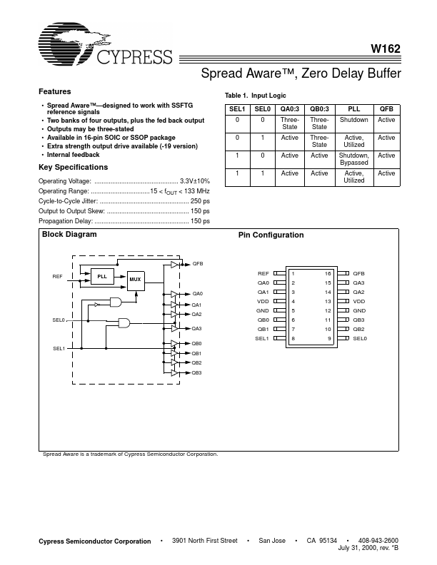
• Spread Aware™—designed to work with SSFTG reference signals • Two banks of four outputs, plus the fed back output • Outputs may be three-stated • Available in 16-pin SOIC or SSOP package • Extra strength output drive available (-19 version) • Internal feedback Table 1. Input Logic SEL1 0 0 1 1 SEL0 0 1 0 1 QA0:3 ThreeState Active Active Active QB0:3 ThreeState ThreeState Active Active PLL Shutdown Active, Utilized Shutdown, Bypassed Active, Utilized QFB Active Active Active Active
Key Specifications
Operating Voltage: ............................................... 3.3V±10% Operating Range: .................................15 < fOUT < 133 MHz Cycle-to-Cycle Jitter: ..................................................
 W162 Datasheet