Description
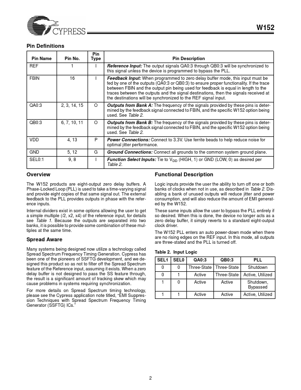
Reference Input: The output signals QA0:3 through QB0:3 will be synchronized to this signal unless the device is programmed to bypass the PLL.
Feedback Input: When programmed to zero delay buffer mode, this input must be fed by one of the outputs (QA0:3 or QB0:3) to ensure proper functionality.
Features
- Spread Aware™.
- designed to work with SSFTG reference signals.
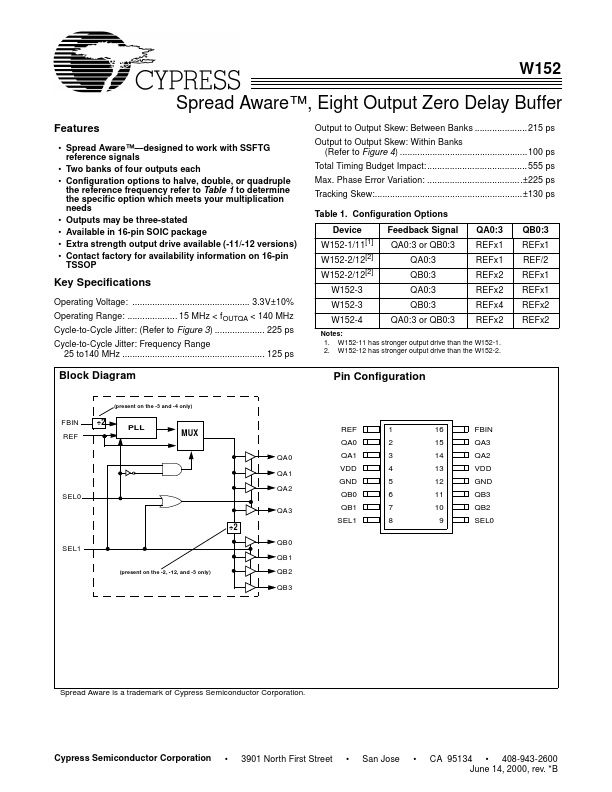
- Two banks of four outputs each.
- Configuration options to halve, double, or quadruple the reference frequency refer to Table 1 to determine the specific option which meets your multiplication needs.
- Outputs may be three-stated.
- Available in 16-pin SOIC package.
- Extra strength output drive available (-11/-12 versions).
- Contact factory for availability information on.
 W152 Datasheet