Datasheet Details
| Part number | GVT7C1362A |
|---|---|
| Manufacturer | Cypress (Infineon) |
| File Size | 793.06 KB |
| Description | 256K x 36 / 512K x 18 Pipelined SRAM |
| Datasheet |
 GVT7C1362A Datasheet GVT7C1362A Datasheet
|
|
|
Download the GVT7C1362A datasheet PDF. This datasheet also covers the GVT71256D36 variant, as both devices belong to the same 256k x 36 / 512k x 18 pipelined sram family and are provided as variant models within a single manufacturer datasheet.
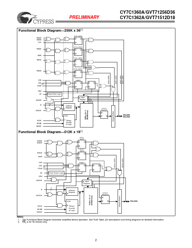
The Cypress Synchronous Burst SRAM family employs high-speed, low-power CMOS designs using advanced triple-layer polysilicon, double-layer metal technology.
Each memory cell consists of four transistors and two high-valued resistors.
| Part number | GVT7C1362A |
|---|---|
| Manufacturer | Cypress (Infineon) |
| File Size | 793.06 KB |
| Description | 256K x 36 / 512K x 18 Pipelined SRAM |
| Datasheet |
GVT7C1362A Datasheet
|
|
|
|
| Part Number | Description | Manufacturer |
|---|
| Part Number | Description |
|---|---|
| GVT7C1360A | 256K x 36 / 512K x 18 Pipelined SRAM |
| GVT7C1361A | 256K x 36 / 512K x 18 Sunchronous Burse Flowthrough SRAM |
| GVT7C1363A | 256K x 36 / 512K x 18 Sunchronous Burse Flowthrough SRAM |
| GVT7C1366A | 256K X 36/512K X 18 Pipelined SRAM |
| GVT7C1367A | 256K X 36/512K X 18 Pipelined SRAM |
The following content is an automatically extracted verbatim text from the original manufacturer datasheet and is provided for reference purposes only.