Datasheet Details
| Part number | GVT7C1359A |
|---|---|
| Manufacturer | Cypress (Infineon) |
| File Size | 283.14 KB |
| Description | 256K X 18 Synchronous-pipelined Cache Tag RAM |
| Datasheet |
 GVT7C1359A Datasheet GVT7C1359A Datasheet
|
|
|
Download the GVT7C1359A datasheet PDF. This datasheet also covers the GVT71256T18 variant, as both devices belong to the same 256k x 18 synchronous-pipelined cache tag ram family and are provided as variant models within a single manufacturer datasheet.
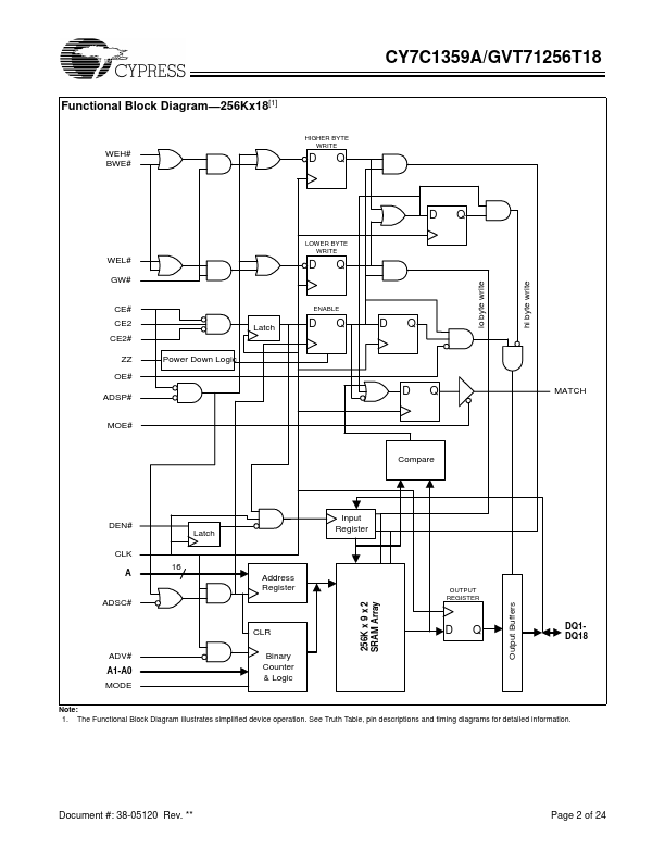
The Cypress Synchronous Burst SRAM family employs high-speed, low power CMOS designs using advanced triple-layer polysilicon, double-layer metal technology.
Each memory cell consists of four transistors and two high valued resistors.
| Part number | GVT7C1359A |
|---|---|
| Manufacturer | Cypress (Infineon) |
| File Size | 283.14 KB |
| Description | 256K X 18 Synchronous-pipelined Cache Tag RAM |
| Datasheet |
GVT7C1359A Datasheet
|
|
|
|
| Part Number | Description | Manufacturer |
|---|
| Part Number | Description |
|---|---|
| GVT7C1354A | 256Kx36/512Kx18 Pipelined SRAM |
| GVT7C1355A | 256K x 36 / 512K x 18 Flow Thru SRAM |
| GVT7C1356A | 256Kx36/512Kx18 Pipelined SRAM |
| GVT7C1357A | 256K x 36 / 512K x 18 Flow Thru SRAM |
| GVT7C1325A | 256K x 18 Synchronous Flow Through Burst SRAM |
The following content is an automatically extracted verbatim text from the original manufacturer datasheet and is provided for reference purposes only.