Datasheet Details
| Part number | GVT7C1356A |
|---|---|
| Manufacturer | Cypress (Infineon) |
| File Size | 597.12 KB |
| Description | 256Kx36/512Kx18 Pipelined SRAM |
| Datasheet |
 GVT7C1356A Datasheet GVT7C1356A Datasheet
|
|
|
Download the GVT7C1356A datasheet PDF. This datasheet also covers the GVT71256ZC36 variant, as both devices belong to the same 256kx36/512kx18 pipelined sram family and are provided as variant models within a single manufacturer datasheet.
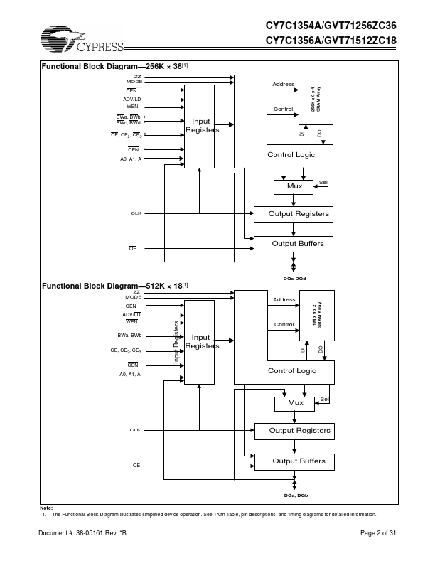
The CY7C1354A/GVT71256ZC36 and CY7C1356A/ GVT71512ZC18 SRAMs are designed to eliminate dead cycles when transitioning from Read to Write or vice versa.
These SRAMs are optimized for 100% bus utilization and achieve Zero Bus Latency (ZBL)/No Bus Latency (NoBL).
| Part number | GVT7C1356A |
|---|---|
| Manufacturer | Cypress (Infineon) |
| File Size | 597.12 KB |
| Description | 256Kx36/512Kx18 Pipelined SRAM |
| Datasheet |
GVT7C1356A Datasheet
|
|
|
|
| Part Number | Description | Manufacturer |
|---|
| Part Number | Description |
|---|---|
| GVT7C1354A | 256Kx36/512Kx18 Pipelined SRAM |
| GVT7C1355A | 256K x 36 / 512K x 18 Flow Thru SRAM |
| GVT7C1357A | 256K x 36 / 512K x 18 Flow Thru SRAM |
| GVT7C1359A | 256K X 18 Synchronous-pipelined Cache Tag RAM |
| GVT7C1325A | 256K x 18 Synchronous Flow Through Burst SRAM |
The following content is an automatically extracted verbatim text from the original manufacturer datasheet and is provided for reference purposes only.