Datasheet Details
| Part number | CY7C1512 |
|---|---|
| Manufacturer | Cypress (now Infineon) |
| File Size | 317.62 KB |
| Description | 64K x 8 Static RAM |
| Datasheet |
 CY7C1512 Datasheet CY7C1512 Datasheet
|
|
|
| Part number | CY7C1512 |
|---|---|
| Manufacturer | Cypress (now Infineon) |
| File Size | 317.62 KB |
| Description | 64K x 8 Static RAM |
| Datasheet |
CY7C1512 Datasheet
|
|
|
|
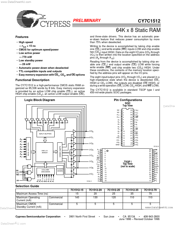
The CY7C1512 is a high-performance CMOS static RAM organized as 65,536 words by 8 bits.
Easy memory expansion is provided by an active LOW chip enable (CE1), an active HIGH chip enable (CE2), an active LOW output enable (OE), Logic Block Diagram Pin Configurations SOIC Top View NC NC A14 A12 A7 A6 A5 A4 A3 A2 A1 A0 I/O0 I/O1 I/O2 GND A11 A9 A8 A13 WE CE2 A15 VCC NC NC A14 A12 A7 A6 A5 A4 1 2 3 4 5 6 7 8 9 10 11 12 13 14 15 16 VCC A15 CE2 WE A13 A8 A9 A11 OE A10 CE1 I/O7 I/O6 I/O5 I/O4 I/O3 32 31 30 29 28 27 26 25 24 23 22 21 20 19 18 17 DataShee DataSheet4U.com I/O0 INPUT BUFFER A0 A1 A2 A3 A4 A5 A6 A7 I/O1 I/O2 64K x 8
www.DataSheet4U.com 1CY 7C15 12 PRELIMINARY CY7C1512 64K x 8 Static.
| Part Number | Description |
|---|---|
| CY7C1512AV18 | 72-Mbit QDR-II SRAM 2-Word Burst Architecture |
| CY7C1512KV18 | 72-Mbit QDR II SRAM Two-Word Burst Architecture |
| CY7C1512V18 | 1.8V Synchronous Pipelined SRAM |
| CY7C1510AV18 | 72-Mbit QDR-II SRAM 2-Word Burst Architecture |
| CY7C1510V18 | 1.8V Synchronous Pipelined SRAM |
| CY7C1511AV18 | 72-Mbit QDR-II SRAM 4-Word Burst Architecture |
| CY7C1511JV18 | 72-Mbit QDR-II SRAM 4-Word Burst Architecture |
| CY7C1511KV18 | (CY7C15xxKV18) 72-Mbit QDR II SRAM 4-Word Burst Architecture |
| CY7C1511V18 | (CY7C15xxV18) SRAM 4-Word Burst Architecture |
| CY7C1513AV18 | 72-Mbit QDR-II SRAM 4-Word Burst Architecture |