CY7C1486V33 Overview
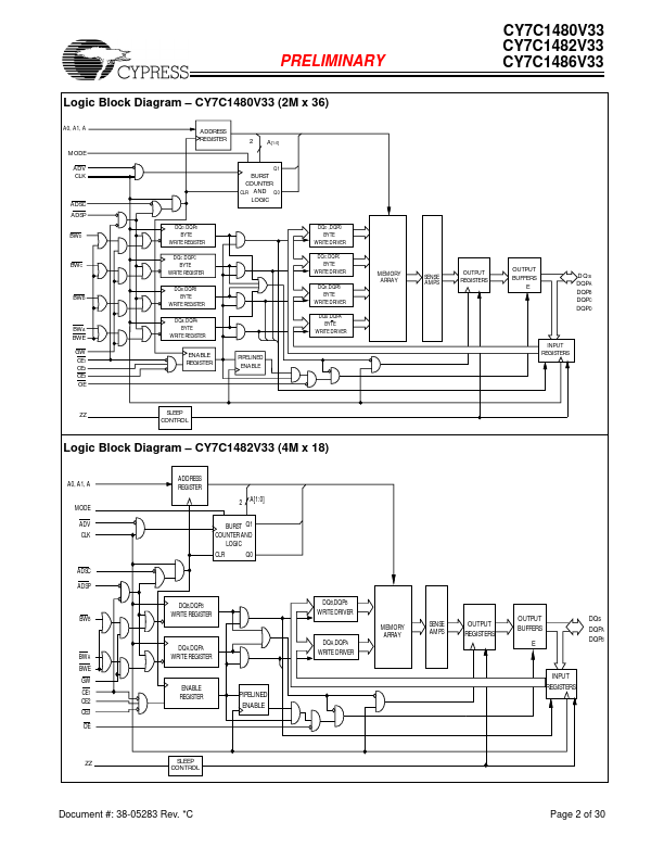
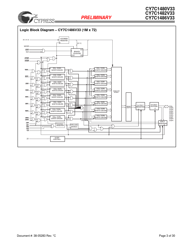
All synchronous inputs are gated by registers controlled by a positive-edge-triggered Clock Input (CLK). The synchronous inputs include all addresses, all data inputs, address-pipelining Chip Enable (CE1), depth-expansion Chip Enables (CE2 and CE3), Burst Control inputs (ADSC, ADSP, and ADV), Write Enables (BWX, and BWE), and Global Write (GW). Asynchronous inputs include the Output Enable (OE) and the ZZ pin.
CY7C1486V33 Key Features
- Supports bus operation up to 250 MHz
- Available speed grades are 250, 200,167 MHz
- Registered inputs and outputs for pipelined operation
- 3.3V core power supply
- 2.5V / 3.3V I/O operation
- Fast clock-to-output times
- 3.0 ns (for 250-MHz device)
- 3.0 ns (for 200-MHz device)
- 3.4 ns (for 167-MHz device)
- Provide high-performance 3-1-1-1 access rate