CY7C1474V33
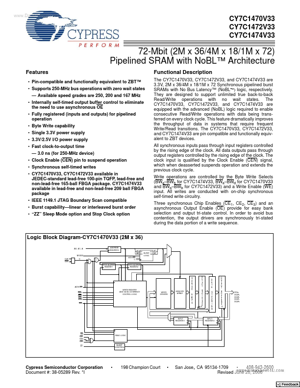
Key Features
- Pin-compatible and functionally equivalent to ZBT™
- Supports 250-MHz bus operations with zero wait states - Available speed grades are 250, 200 and 167 MHz
- Internally self-timed output buffer control to eliminate the need to use asynchronous OE
- Fully registered (inputs and outputs) for pipelined operation
- Byte Write capability
- Single 3.3V power supply
- 3.3V/2.5V I/O power supply
- Fast clock-to-output time - 3.0 ns (for 250-MHz device)
- Clock Enable (CEN) pin to suspend operation
- Synchronous self-timed writes