The following content is an automatically extracted verbatim text
from the original manufacturer datasheet and is provided for reference purposes only.
View original datasheet text
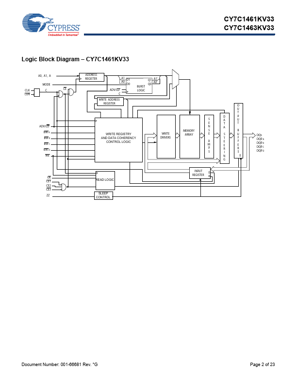
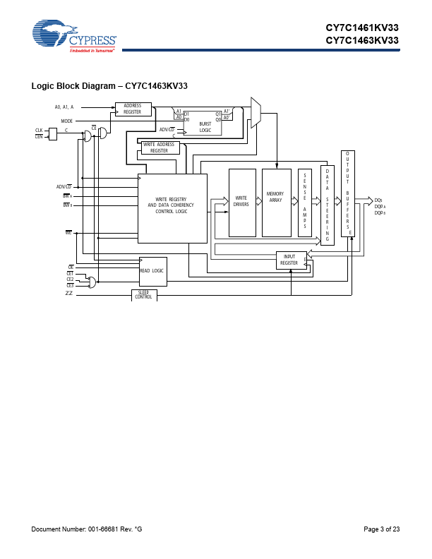
CY7C1461KV33 CY7C1463KV33
36-Mbit (1M × 36/2M × 18) Flow-Through SRAM with NoBL™ Architecture
36-Mbit (1M × 36/2M × 18) Flow-Through SRAM with NoBL™ Architecture
Features
■ No Bus Latency™ (NoBL™) architecture eliminates dead cycles between write and read cycles
■ Supports up to 133 MHz bus operations with zero wait states ❐ Data is transferred on every clock
■ Pin compatible and functionally equivalent to ZBT™ devices
■ Internally self timed output buffer control to eliminate the need to use OE
■ Registered inputs for flow through operation
■ Byte write capability
■ 3.3 V and 2.5 V I/O power supply
■ Fast clock-to-output times ❐ 6.
 CY7C1461KV33 Datasheet