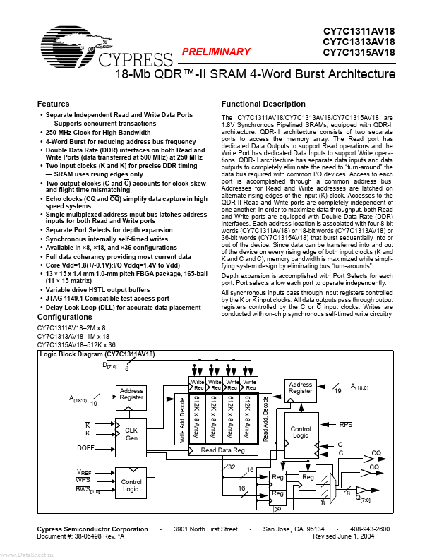
• Part: CY7C1315AV18
  • Description: (CY7C131xAV18) 18-Mb QDRTM-II SRAM 4-Word Burst Architecture
  • Manufacturer: Cypress
  • Size: 356.67 KB
Download CY7C1315AV18 Datasheet PDF
Cypress
CY7C1315AV18
CY7C1315AV18 is (CY7C131xAV18) 18-Mb QDRTM-II SRAM 4-Word Burst Architecture manufactured by Cypress.
- Part of the CY7C1311AV18 comparator family.
PRELIMINARY CY7C1311AV18 CY7C1313AV18 CY7C1315AV18 18-Mb QDR™-II SRAM 4-Word Burst Architecture Features - Separate Independent Read and Write Data Ports - Supports concurrent transactions - 250-MHz Clock for High Bandwidth - 4-Word Burst for reducing address bus frequency - Double Data Rate (DDR) interfaces on both Read and Write Ports (data transferred at 500 MHz) at 250 MHz - Two input clocks (K and K) for precise DDR timing - SRAM uses rising edges only - Two output clocks (C and C) accounts for clock skew and flight time mismatching - Echo clocks (CQ and CQ) simplify data capture in high speed systems - Single multiplexed address input bus latches address inputs for both Read and Write ports - Separate Port Selects for depth expansion - Synchronous internally self-timed writes - Available in ×8, ×18, and ×36 configurations - Full data coherancy providing most current data - Core Vdd=1.8(+/-0.1V);I/O Vddq=1.4V to Vdd) - 13 × 15 x 1.4 mm 1.0-mm pitch FBGA package, 165-ball (11 × 15 matrix) - Variable drive HSTL output buffers - JTAG 1149.1 patible test access port - Delay Lock Loop (DLL) for accurate data placement Functional Description The CY7C1311AV18/CY7C1313AV18/CY7C1315AV18 are 1.8V Synchronous Pipelined SRAMs, equipped with QDR-II architecture. QDR-II architecture consists of two separate ports to access the memory array. The Read port has dedicated Data Outputs to support Read operations and the Write Port has dedicated Data Inputs to support Write operations. QDR-II architecture has separate data inputs and data outputs to pletely eliminate the need to “turn-around” the data bus required with mon I/O devices. Access to each port is acplished through a mon address bus. Addresses for Read and Write addresses are latched on alternate rising edges of the input (K) clock. Accesses to the QDR-II Read and Write ports are pletely independent of one another. In order to maximize data throughput, both Read and Write ports are equipped with...