CY7C1308DV25
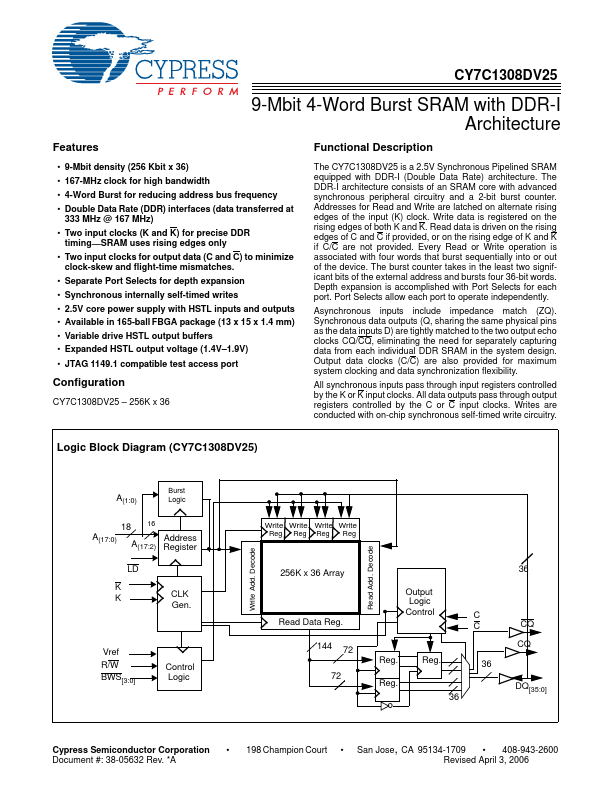
Overview
- 9-Mbit density (256 Kbit x 36)
- 167-MHz clock for high bandwidth
- 4-Word Burst for reducing address bus frequency
- Double Data Rate (DDR) interfaces (data transferred at 333 MHz @ 167 MHz)
- Two input clocks (K and K) for precise DDR timing-SRAM uses rising edges only
- Two input clocks for output data (C and C) to minimize clock-skew and flight-time mismatches.
- Separate Port Selects for depth expansion
- Synchronous internally self-timed writes
- 2.5V core power supply with HSTL inputs and outputs
- Available in 165-ball FBGA package (13 x 15 x 1.4 mm)