Datasheet4U Logo Datasheet4U.com

CY7C12701KV18 - 1.8 V synchronous pipelined SRAM

Download the CY7C12701KV18 datasheet PDF. This datasheet also covers the CY7C12661KV18 variant, as both devices belong to the same 1.8 v synchronous pipelined sram family and are provided as variant models within a single manufacturer datasheet.

Key Features

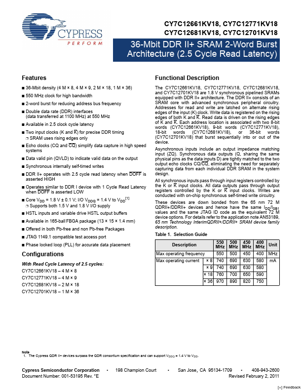
  • 36-Mbit density (4 M × 8, 4 M × 9, 2 M × 18, 1 M × 36).
  • 550 MHz clock for high bandwidth.
  • 2-word burst for reducing address bus frequency.
  • Double data rate (DDR) interfaces (data transferred at 1100 MHz) at 550 MHz.
  • Available in 2.5 clock cycle latency.
  • Two input clocks (K and K) for precise DDR timing.
  • SRAM uses rising edges only.
  • Echo clocks (CQ and CQ) simplify data capture in high speed systems.
  • Data valid pin (QVLD) to indicate valid data on the.

📥 Download Datasheet

Note: The manufacturer provides a single datasheet file (CY7C12661KV18-CypressSemiconductor.pdf) that lists specifications for multiple related part numbers.

Full PDF Text Transcription (Reference)

The following content is an automatically extracted verbatim text from the original manufacturer datasheet and is provided for reference purposes only.

View original datasheet text
CY7C12661KV18, CY7C12771KV18 CY7C12681KV18, CY7C12701KV18 36-Mbit DDR II+ SRAM 2-Word Burst Architecture (2.5 Cycle Read Latency) 36-Mbit DDR II+ SRAM 2-Word Burst Architecture (2.5 Cycle Read Latency) Features ■ 36-Mbit density (4 M × 8, 4 M × 9, 2 M × 18, 1 M × 36) ■ 550 MHz clock for high bandwidth ■ 2-word burst for reducing address bus frequency ■ Double data rate (DDR) interfaces (data transferred at 1100 MHz) at 550 MHz ■ Available in 2.5 clock cycle latency ■ Two input clocks (K and K) for precise DDR timing ❐ SRAM uses rising edges only ■ Echo clocks (CQ and CQ) simplify data capture in high speed systems ■ Data valid pin (QVLD) to indicate valid data on the output ■ Synchronous internally self-timed writes ■ DDR II+ operates with 2.