CY6264
Overview
- 55, 70 ns access times
- CMOS for optimum speed/power
- Easy memory expansion with CE1, CE2, and OE features
- TTL-compatible inputs and outputs
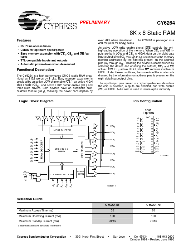
- Automatic power-down when deselected over 70% when deselected. The CY6264 is packaged in a 450-mil (300-mil body) SOIC. An active LOW write enable signal (WE) controls the writing/reading operation of the memory. When CE1 and WE inputs are both LOW and CE2 is HIGH, data on the eight data input/output pins (I/O0 through I/O7) is written into the memory location addressed by the address present on the address pins (A0 through A12). Reading the device is accomplished by selecting the device and enabling the outputs, CE1 and OE active LOW, CE2 active HIGH, while WE remains inactive or HIGH. Under these conditions, the contents of the location addressed by the information on address pins is present on the eight data input/output pins. The input/output pins remain in a high-impedance state unless the chip is selected, outputs are enabled, and write enable (WE) is HIGH. A die coat is used to insure alpha immunity. Functional Description The CY6264 is a high-performance CMOS static RAM organized as 8192 words by 8 bits. Easy memory expansion is provided by an active LOW chip enable (CE1), an active HIGH chip enable (CE2), and active LOW output enable (OE) and three-state drivers. Both devices have an automatic power-down feature (CE1), reducing the power consumption by Logic Block Diagram