CY62128
Overview
- 4.5V - 5.5V operation
- CMOS for optimum speed/power
- Low active power (70 ns, LL version) - 330 mW (max.) (60 mA)
- Low standby power (70 ns, LL version) - 110 µW (max.) (20 µA)
- Automatic power-down when deselected
- TTL-compatible inputs and outputs
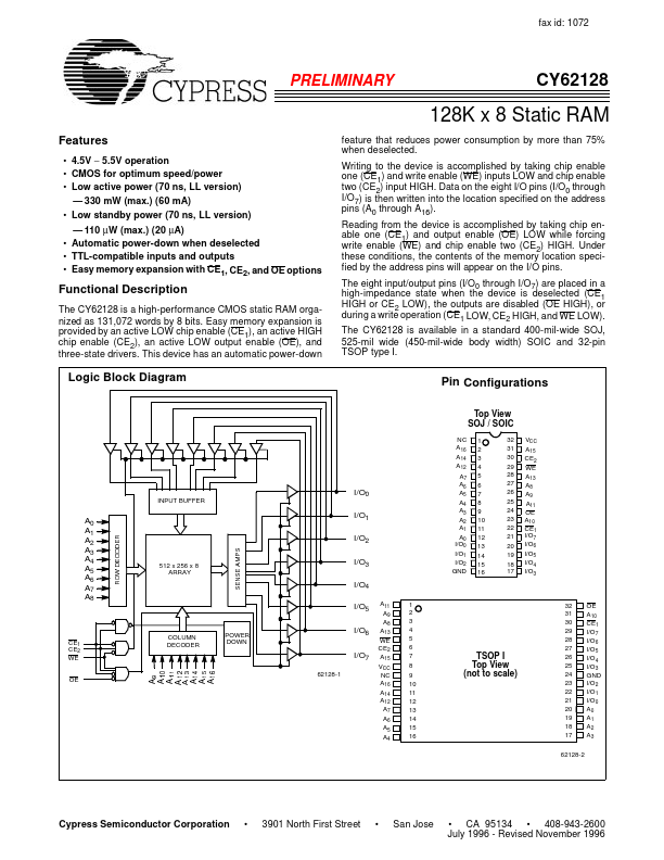
- Easy memory expansion with CE1, CE2, and OE options feature that reduces power consumption by more than 75% when deselected. Writing to the device is accomplished by taking chip enable one (CE1) and write enable (WE) inputs LOW and chip enable two (CE2) input HIGH. Data on the eight I/O pins (I/O0 through I/O7) is then written into the location specified on the address pins (A0 through A16). Reading from the device is accomplished by taking chip enable one (CE1) and output enable (OE) LOW while forcing write enable (WE) and chip enable two (CE2) HIGH. Under these conditions, the contents of the memory location specified by the address pins will appear on the I/O pins. The eight input/output pins (I/O0 through I/O7) are placed in a high-impedance state when the device is deselected (CE1 HIGH or CE2 LOW), the outputs are disabled (OE HIGH), or during a write operation (CE1 LOW, CE2 HIGH, and WE LOW). The CY62128 is available in a standard 400-mil-wide SOJ, 525-mil wide (450-mil-wide body width) SOIC and 32-pin TSOP type I. Functional Description The CY62128 is a high-performance CMOS static RAM organized as 131,072 words by 8 bits. Easy memory expansion is provided by an active LOW chip enable (CE1), an active HIGH chip enable (CE2), an active LOW output enable (OE), and three-state drivers. This device has an automatic power-down Logic Block Diagram