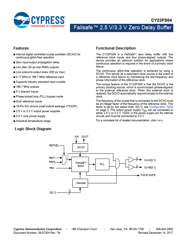
Datasheet4U Logo Datasheet4U.com

CY23FS04 - 2.5V / 3.3V Zero Delay Buffer

Description

The CY23FS04 is a FailSafe zero delay buffer with two reference clock inputs and four phase-aligned outputs.

The device provides an optimum solution for applications where continuous operation is required in the event of a primary clock failure.

Features

  • Internal digital controlled crystal oscillator (DCXO) for continuous glitch-free operation.
  • Zero input-output propagation delay.
  • Low jitter (35 ps max RMS) outputs.
  • Low output-to-output skew (200 ps max).
  • 4.17 MHz to 166.7 MHz reference input.
  • Supports industry standard input crystals.
  • 166.7 MHz outputs.
  • 5 V tolerant Inputs.
  • Phase-locked loop (PLL) bypass mode.
  • Dual reference inputs.
  • 16-Pin thin shrunk small outline package (TSSOP).
  • 2.

📥 Download Datasheet

Full PDF Text Transcription (Reference)

The following content is an automatically extracted verbatim text from the original manufacturer datasheet and is provided for reference purposes only.

View original datasheet text
CY23FS04 Failsafe™ 2.5 V/3.3 V Zero Delay Buffer Failsafe™ 2.5 V/3.3 V Zero Delay Buffer Features ■ Internal digital controlled crystal oscillator (DCXO) for continuous glitch-free operation ■ Zero input-output propagation delay ■ Low jitter (35 ps max RMS) outputs ■ Low output-to-output skew (200 ps max) ■ 4.17 MHz to 166.7 MHz reference input ■ Supports industry standard input crystals ■ 166.7 MHz outputs ■ 5 V tolerant Inputs ■ Phase-locked loop (PLL) bypass mode ■ Dual reference inputs ■ 16-Pin thin shrunk small outline package (TSSOP) ■ 2.5 V or 3.3 V output power supplies ■ 3.
Published: |