CY2302
CY2302 is Frequency Multiplier and Zero Delay Buffer manufactured by Cypress.
Features
- 90 ps typical jitter OUT2
- 200 ps typical jitter OUT1
- 65 ps typical output-to-output skew
- 90 ps typical propagation delay
- Voltage range: 3.3 V±5%, or 5 V±10%
- Output frequency range: 5 MHz to 133 MHz
- Two outputs
- Configuration options allow various multiplications of the reference frequency- refer to Table 1 to determine the specific option which meets your multiplication needs
- Available in 8-pin SOIC package
Frequency Multiplier and Zero Delay Buffer
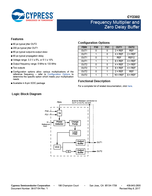
Table 1. Configuration Options
FBIN OUT1 OUT1 OUT1 OUT1 OUT2 OUT2 OUT2 OUT2
FS0 FS1
OUT1
0 0 2 X REF
1 0 4 X REF
1 1 8 X REF
0 0 4 X REF
1 0 8 X REF
0 1 2 X REF
1 1 16 X REF
OUT2 REF 2 X REF REF/2 4 X REF 2 X REF 4 X REF REF 8 X REF
Logic Block Diagram
FBIN
External feedback connection to OUT1 or OUT2, not both
FS0 FS1 ÷Q
IN Reference
Input
Phase...