6116A
Description
Test Conditions Min. VOH VOL VIH VIL IIX IOZ IOS ICC Output HIGHVoltage Output LOW Voltage Input HIGH Voltage Input LOW Voltage [3] Input Load Current Output Leakage Current Output Short Circuit Current [4] VCC Operating p g S l Current C Supply VCC = Min., I OH = -4.0 mA VCC = Min., I OL = 8.0 mA 2.4 0.4 2.2 -0.5 VCC 0.8 +10 +10 -300 100 2.4 0.4 2.2 -0.5 -10 -10 VCC 0.8 +10 +10 -300 100 125 100 40 20 40 20 20 20 20 2.4 0.4 2.2 -0.5 -10 -10 VCC 0.8 +10 +10 -300 80 100 20 20 20 20 V V V V GND < VI < VCC GND < VI < VCC, Output Disabled VCC = Max., V OUT = GND VCC = Max.
Key Features
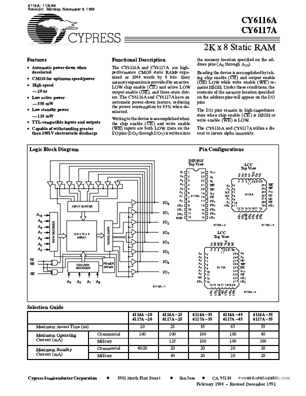
- D Automatic powerĆdown when deselected CMOS for optimum speed/power High speed Ċ 20 ns Low active power Ċ 550 mW Low standby power Ċ 110 mW TTLĆcompatible inputs and outputs Capable of withstanding greater than 2001V electrostatic discharge The CY6116A and CY6117A are highĆ performance CMOS static RAMs orgaĆ nized as 2048 words by 8 bits. Easy memoryexpansionisprovidedbyanactive LOW chip enable (CE) and active LOW output enable (OE), and threeĆstate drivĆ ers. The CY6116A and CY6117A have an automatic powerĆdown feature, reducing the power consumption by 83% when deĆ selected. Writingtothedeviceisaccomplishedwhen the chip enable (CE) and write enable (WE) inputs are both LOW. Data on the I/Opins(I/O 0 throughI/O 7)iswritteninto Functional Description the memory location specified on the adĆ dress pins (A 0 through A 10). ReadingthedeviceisaccomplishedbytakĆ ing chip enable (CE) and output enable (OE) LOW while write enable (WE ) reĆ mains HIGH.Undertheseconditions,the contents of the memory location specified on the address pins will appear on the I/O pins. The I/O pins remain in highĆimpedance state when chip enable (CE ) is HIGH or write enable (WE) is LOW. The CY6116A and CY6117A utilize a die coat to insure alpha immunity. 2K x 8 Static RAM