Datasheet Details
| Part number | CY23FS08 |
|---|---|
| Manufacturer | Cypress (Infineon) |
| File Size | 309.98 KB |
| Description | 2.5V / 3.3V Zero Delay Buffer |
| Datasheet |
 CY23FS08 Datasheet CY23FS08 Datasheet
|
|
|
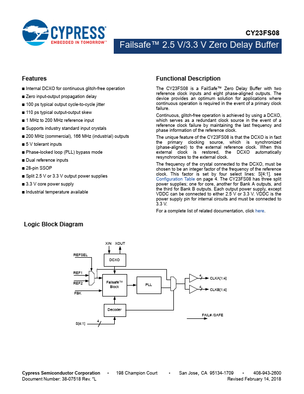
The CY23FS08 is a FailSafe™ Zero Delay Buffer with two reference clock inputs and eight phase-aligned outputs.
| Part number | CY23FS08 |
|---|---|
| Manufacturer | Cypress (Infineon) |
| File Size | 309.98 KB |
| Description | 2.5V / 3.3V Zero Delay Buffer |
| Datasheet |
CY23FS08 Datasheet
|
|
|
|
| Part Number | Description | Manufacturer |
|---|---|---|
| CY23FS04 | 2.5V / 3.3V Zero Delay Buffer | Cypress Semiconductor |
| CY2300 | Phase-Aligned Clock Multiplier | Cypress Semiconductor |
| CY2302 | Frequency Multiplier and Zero Delay Buffer | Cypress Semiconductor |
| CY2303 | Phase-Aligned Clock Multiplier | Cypress Semiconductor |
| CY2305C | Zero Delay Buffers | Cypress Semiconductor |
| Part Number | Description |
|---|---|
| CY23FP12 | 200MHz Field Programmable Zero Delay Buffer |
| CY2304 | 3.3V Zero Delay Buffer |
| CY2304NZ | Four Output PCI-X and General Purpose Buffer |
| CY2305 | Low Cost 3.3 V Zero Delay Buffer |
| CY2308 | 3.3V Zero Delay Buffer |
The following content is an automatically extracted verbatim text from the original manufacturer datasheet and is provided for reference purposes only.