Datasheet4U Logo Datasheet4U.com

CY23EP05 - 5 Output Zero Delay Buffer

Description

The CY23EP05 is a 2.5 V or 3.3 V zero delay buffer designed to distribute low-jitter high-speed clocks and is available in a 8-pin SOIC package.

It accepts one reference input, and drives out five low-skew clocks.

Features

  • 10 MHz to 220 MHz maximum operating range.
  • Zero input-output propagation delay, adjustable by loading on CLKOUT pin.
  • Multiple low-skew outputs.
  • 30 ps typical output-output skew.
  • One input drives five outputs.
  • 22 ps typical cycle-to-cycle jitter.
  • 13 ps typical period jitter.
  • Standard and high drive strength options.
  • Available in space-saving 150-mil SOIC package.
  • 3.3 V or 2.5 V operation.
  • Industrial temperature available Functional Descript.

📥 Download Datasheet

Full PDF Text Transcription (Reference)

The following content is an automatically extracted verbatim text from the original manufacturer datasheet and is provided for reference purposes only.

View original datasheet text
CY23EP05 2.5 V or 3.3 V,10–220 MHz, Low Jitter, 5 Output Zero Delay Buffer 2.5 V or 3.3 V,10–220 MHz, Low Jitter, 5 Output Zero Delay Buffer Features ■ 10 MHz to 220 MHz maximum operating range ■ Zero input-output propagation delay, adjustable by loading on CLKOUT pin ■ Multiple low-skew outputs ❐ 30 ps typical output-output skew ❐ One input drives five outputs ■ 22 ps typical cycle-to-cycle jitter ■ 13 ps typical period jitter ■ Standard and high drive strength options ■ Available in space-saving 150-mil SOIC package ■ 3.3 V or 2.5 V operation ■ Industrial temperature available 
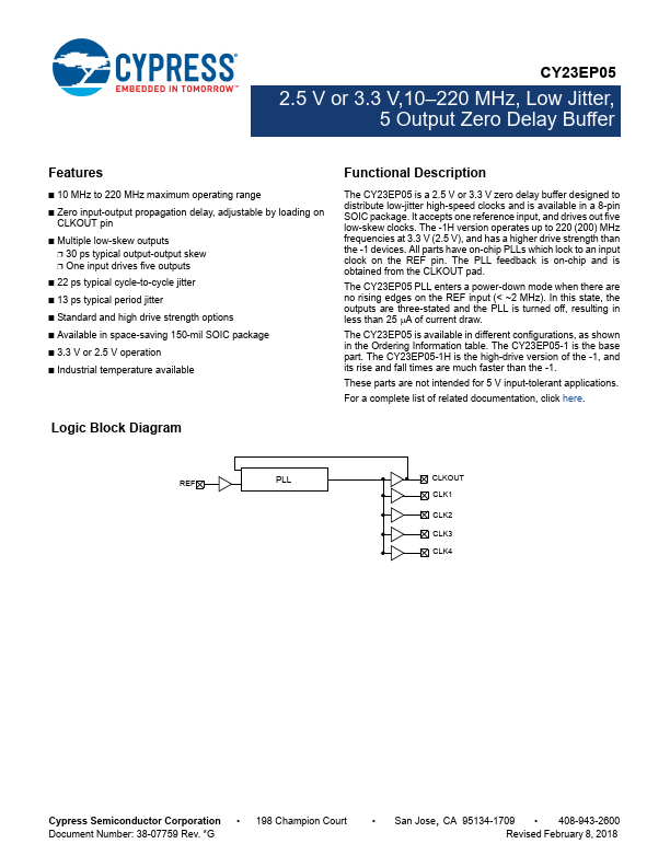
Functional Description The CY23EP05 is a 2.5 V or 3.3 V zero delay buffer designed to distribute low-jitter high-speed clocks and is available in a 8-pin SOIC package.
Published: |