CDZ55B51
FEATURES
- Silicon planar power zener diodes
- SMD chip pattern, available in various dimension included 0805 (CDZ55B-S series)
- Leadfree and Ro HS pliance ponents
MECHANICAL CHARACTERISTICS
- Size: 1206
- Weight: approx. 10mg
- Marking: Zener voltage & cathode terminal
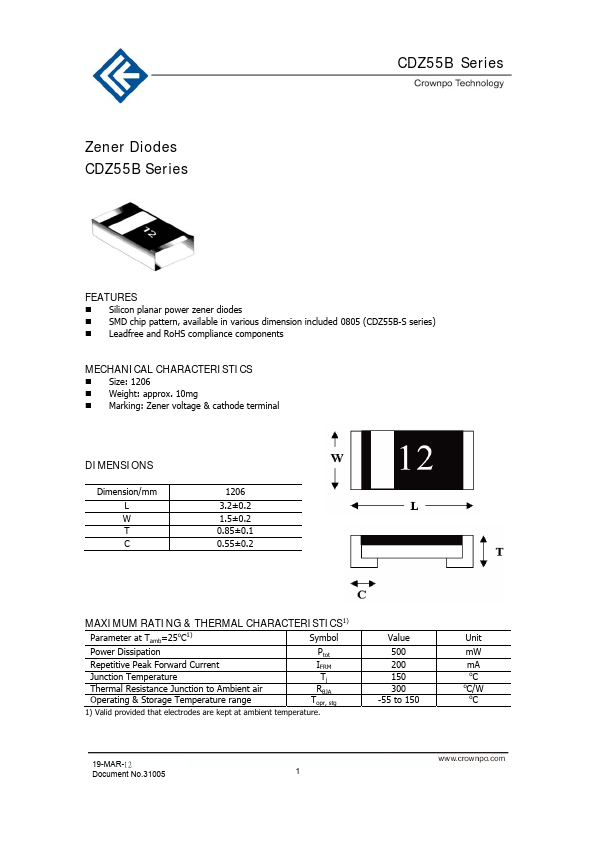
DIMENSIONS
Dimension/mm L W T C
3.2±0.2 1.5±0.2 0.85±0.1 0.55±0.2
MAXIMUM RATING & THERMAL CHARACTERISTICS1)
Parameter at Tamb=25o C1)
Symbol
Power Dissipation
Repetitive Peak Forward Current
Junction Temperature Thermal Resistance Junction to Ambient air Operating & Storage Temperature range
Ptot
IFRM
Tj RθJA Topr, stg
1) Valid provided that electrodes are kept at ambient temperature.
Value
500 200 150 300 -55 to 150
Unit m W m A o C o C/W o C
19-MAR-12 Document No.31005
CDZ55B Series
ELECTRICAL CHARACTERISTICS1)
Parameter at Tamb=25o C1)
Forward Voltage at IF=200m A Zener Voltage Tolerance, B=±2%
Symbol VF
1) Valid provided that electrodes are kept at ambient temperature.
Value 1.5 MAX
Unit V
Part...