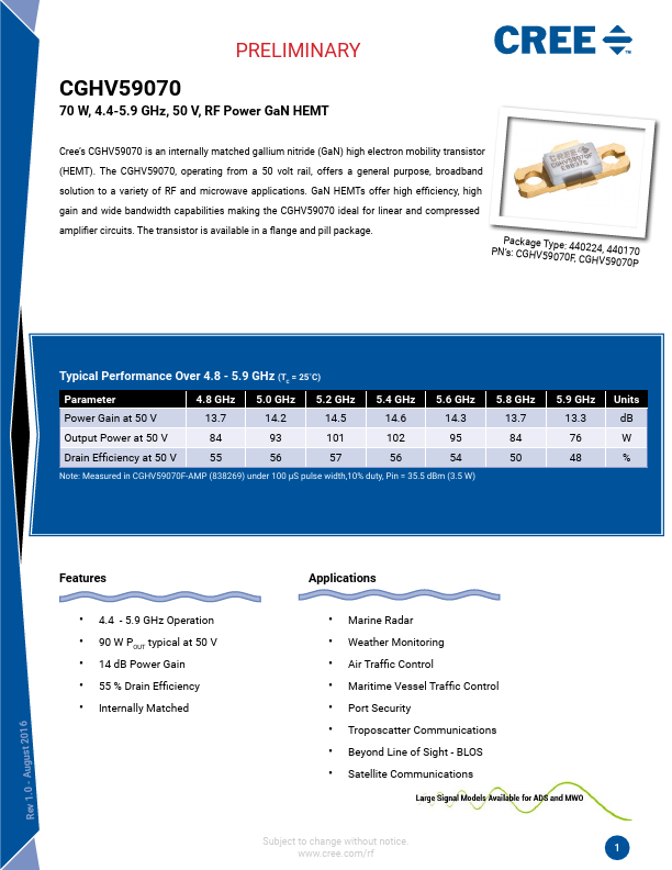
Absolute Maximum Ratings (not simultaneous) at 25˚C Case Temperature
Parameter
Symbol
Rating
Drain-Source Voltage
Gate-to-Source Voltage
Storage Temperature
Operating Junction Temperature
Maximum Forward Gate Current
Maximum Drain Current1
Soldering Temperature2
Screw Torque
VDSS
VGS
TSTG
TJ
IGMAX
IDMAX
TS
τ
150
-10, +2
-65, +150
225
10.4
6.3
245
40
Thermal Resistance, Junction to Case3
RθJC 2.99
Thermal Resistance, Junction to Case3
RθJC 0.85
Case Operating Temperature2
TC -40, +150
Note:
1 Current limit for long term, reliable operation
2 Refer to the Application Note on soldering at www.cree.com/RF/Document-Library
3 Simulated for the CGHV59070F at PDISS = 57.6 CW or PDISS = 70 W Pulsed
4 See also, the Power Dissipation De-rating Curve on Page 8.
Electrical Characteristics (TC = 25˚C)
Units
Volts
Volts
˚C
˚C
mA
A
˚C
in-oz
˚C/W
˚C/W
˚C
Conditions
25˚C
25˚C
25˚C
25˚C
85˚C, CW @ PDISS = 57 W
85˚C, 100 μsec, 10% Duty Cycle @ PDISS = 70 W
Characteristics
Symbol
Min.
Typ.
DC Characteristics1
Gate Threshold Voltage
Saturated Drain Current2
Drain-Source Breakdown
Voltage
VGS(th)
IDS
VBR
-3.8
7.8
150
-2.8
10.4
–
RF Characteristics3 (TC = 25˚C, F0 = 2.5 GHz unless otherwise noted)
Output Power
POUT1
–
100
Output Power
POUT1
–
95
Output Power
POUT1
–
76
Drain Efficiency
EFF1
–
57
Drain Efficiency
EFF2
–
54
Drain Efficiency
EFF3
–
48
Power Gain
PG1 – 14.5
Power Gain
PG2 – 14.3
Power Gain
PG3 – 13.3
Output Mismatch Stress
VSWR
–
–
Dynamic Characteristics
Input Capacitance
CGS
Output Capacitance
CDS
Feedback Capacitance
CGD
Notes:
1 Measured on wafer prior to packaging.
2 Scaled from PCM data.
3 Measured in CGHV59070F-AMP
4 Drain Efficiency = POUT / PDC
–
–
–
36
109
0.26
Max.
-2.3
–
–
–
–
–
–
–
–
–
–
–
5:1
–
–
–
Units
VDC VDS = 10 V, ID = 10.4 mA
A VDS = 6.0 V, VGS = 2.0 V
VDC VGS = -8 V, ID = 10.4 mA
Conditions
W VDD = 50 V, IDQ = 0.15 A, PIN = 35.5 dBm, Freq = 5.2 GHz
W VDD = 50 V, IDQ = 0.15 A, PIN = 35.5 dBm, Freq = 5.55 GHz
W VDD = 50 V, IDQ = 0.15 A, PIN = 35.5 dBm, Freq = 5.9 GHz
% VDD = 50 V, IDQ = 0.15 A, PIN = 35.5 dBm, Freq = 5.2 GHz
% VDD = 50 V, IDQ = 0.15 A, PIN = 35.5 dBm, Freq = 5.55 GHz
% VDD = 50 V, IDQ = 0.15 A, PIN = 35.5 dBm, Freq = 5.9 GHz
dB VDD = 50 V, IDQ = 0.15 A, PIN = 35.5 dBm, Freq = 5.2 GHz
dB VDD = 50 V, IDQ = 0.15 A, PIN = 35.5 dBm, Freq = 5.55 GHz
dB VDD = 50 V, IDQ = 0.15 A, PIN = 35.5 dBm, Freq = 5.9 GHz
Y No damage at all phase angles, VDD = 50 V, IDQ = 0.15A, PIN = 35.5 dBm Pulsed
pF VDS = 50 V, Vgs = -8 V, f = 1 MHz
Copyright © 2016 Cree, Inc. All rights reserved. The information in this document is subject to change without notice. Cree and the Cree logo are
registered trademarks of Cree, Inc.
2 CGHV59070 Rev 1.0
Cree, Inc.
4600 Silicon Drive
Durham, North Carolina, USA 27703
USA Tel: +1.919.313.5300
Fax: +1.919.869.2733
www.cree.com/rf