Datasheet Details
| Part number | CGHV40030 |
|---|---|
| Manufacturer | Cree |
| File Size | 2.29 MB |
| Description | GaN HEMT |
| Datasheet |
 CGHV40030 Datasheet CGHV40030 Datasheet
|
|
|
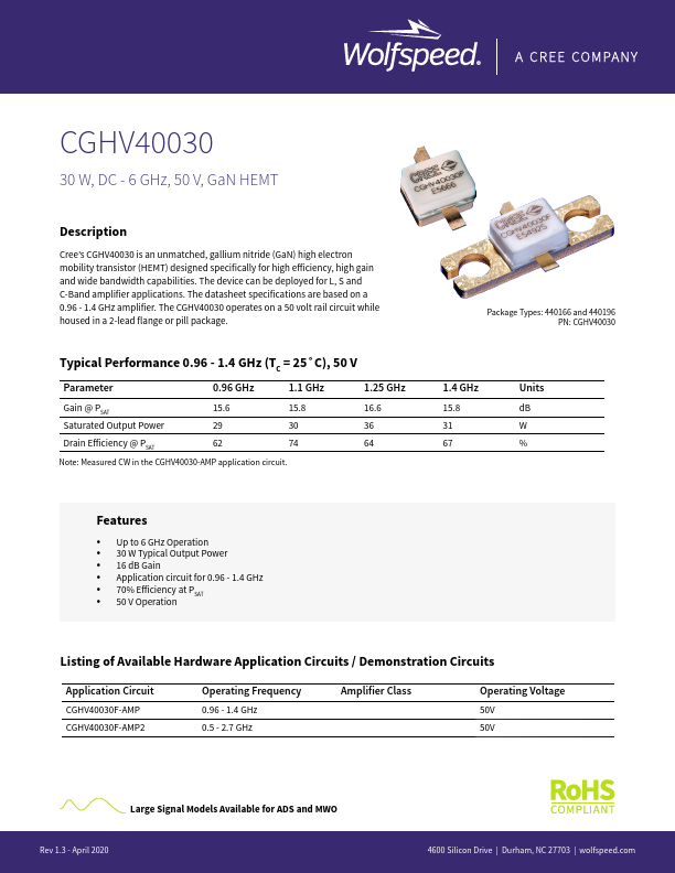
Cree’s CGHV40030 is an unmatched, gallium nitride (GaN) high electron mobility transistor (HEMT) designed specifically for high efficiency, high gain and wide bandwidth capabilities.
The device can be deployed for L, S and C-Band amplifier applications.
The datasheet specifications are based on a 0.
| Part number | CGHV40030 |
|---|---|
| Manufacturer | Cree |
| File Size | 2.29 MB |
| Description | GaN HEMT |
| Datasheet |
CGHV40030 Datasheet
|
|
|
|