The following content is an automatically extracted verbatim text
from the original manufacturer datasheet and is provided for reference purposes only.
View original datasheet text
PRELIMINARY
CGHV35060MP
60W, 2700-3500 MHz, 50V, GaN HEMT for S Band Radar and LTE base stations
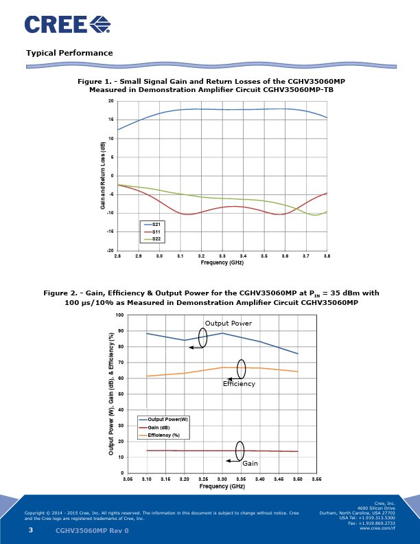
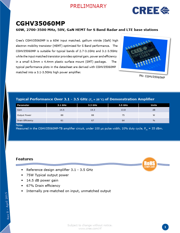
Cree’s CGHV35060MP is a 60W input matched, gallium nitride (GaN) high electron mobility transistor (HEMT) optimized for S Band performance. The CGHV35060MP is suitable for typical bands of 2.7-3.1GHz and 3.1-3.5GHz while the input matched transistor provides optimal gain, power and efficiency in a small 6.5mm x 4.4mm plastic surface mount (SMT) package. The typical performance plots in the datasheet are derived with CGHV35060MP matched into a 3.1-3.5GHz high power amplifier.
PN: CGHV35060MP
Typical Performance Over 3.1 - 3.5 GHz (TC = 25˚C) of Demonstration Amplifier
Parameter
3.1 GHz
3.3 GHz
3.5 GHz
Units
Gain
14.5
14.3
13.
 CGHV35060MP Datasheet