Datasheet Summary
6 W, DC
- 15 GHz, 40V, GaN HEMT
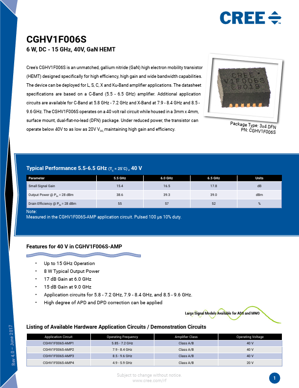
Cree’s CGHV1F006S is an unmatched, gallium nitride (GaN) high electron mobility transistor (HEMT) designed specifically for high efficiency, high gain and wide bandwidth capabilities. The device can be deployed for L, S, C, X and Ku-Band amplifier applications. The datasheet specifications are based on a C-Band (5.5
- 6.5 GHz) amplifier. Additional application circuits are available for C-Band at 5.8 GHz
- 7.2 GHz and X-Band at 7.9
- 8.4 GHz and 8.5 9.6 GHz. The CGHV1F006S operates on a 40 volt rail circuit while housed in a 3mm x 4mm, surface mount, dual-flat-no-lead (DFN) package. Under reduced power, the transistor can operate below 40V to as...