CGH40180PP Datasheet Text
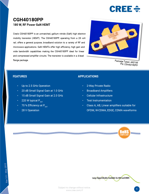
CGH40180PP
180 W, RF Power GaN HEMT
Cree’s CGH40180PP is an unmatched, gallium nitride (GaN) high electron mobility transistor (HEMT). The CGH40180PP, operating from a 28 volt rail, offers a general purpose, broadband solution to a variety of RF and microwave applications. GaN HEMTs offer high efficiency, high gain and wide bandwidth capabilities making the CGH40180PP ideal for linear and pressed amplifier circuits. The transistor is available in a 4-lead flange package.
PackaPgNe:TCyGpeHs4:04148001P9P9
Features
- Up to 2.5 GHz Operation
- 20 dB Small Signal Gain at 1.0 GHz
- 15 dB Small Signal Gain at 2.0 GHz
- 220 W typical PSAT
- 70 % Efficiency at PSAT
- 28 V Operation
APPLICATIONS
- 2-Way Private Radio
- Broadband Amplifiers
- Cellular Infrastructure
- Test Instrumentation
- Class A, AB, Linear amplifiers suitable for
OFDM, W-CDMA, EDGE, CDMA waveforms
Rev 3.0
- May 2015
Subject to change without notice....