CGH35240F
CGH35240F is GaN HEMT manufactured by Cree.
240 W, 3100-3500 MHz, 50-ohm Input/Output Matched, GaN HEMT for S-Band Radar Systems
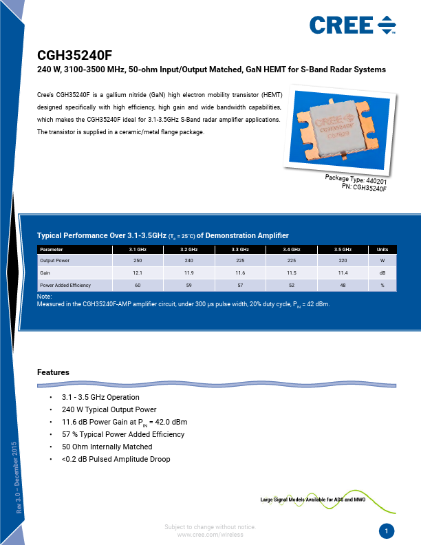
Cree’s CGH35240F is a gallium nitride (GaN) high electron mobility transistor (HEMT) designed specifically with high efficiency, high gain and wide bandwidth capabilities, which makes the CGH35240F ideal for 3.1-3.5GHz S-Band radar amplifier applications. The transistor is supplied in a ceramic/metal flange package.
PackaPgeN:TCypGeH: 3454204200F1
Typical Performance Over 3.1-3.5GHz (TC = 25˚C) of Demonstration Amplifier
Parameter
3.1 GHz
3.2 GHz
3.3 GHz
3.4 GHz
Output Power
250 240 225 225
3.5 GHz 220
Gain
Power Added Efficiency
Note:...