CJ1012-G Description
MOSFET CJ1012-G N-Channel RoHS Device.
CJ1012-G Key Features
- High-Side Switching
- Low On-Resistance
- Low Threshold
- Fast Switching Speed
- ESD protected up to 2KV
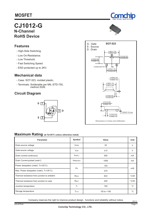
- Case: SOT-323, molded plastic
- Terminals: Solderable per MIL-STD-750
CJ1012-G is MOSFET manufactured by Comchip.
| Manufacturer | Part Number | Description |
|---|---|---|
| CJ1012 | N-Channel MOSFET | |
| ZPSEMI ZPSEMI |
CJ1012 | N-Channel Power MOSFET |
MOSFET CJ1012-G N-Channel RoHS Device.