CMH20N50 Overview
Description
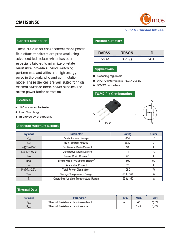
Product Summery These N-Channel enhancement mode power field effect transistors are produced using advanced technology which has been especially tailored to minimize on-state resistance, provide superior switching performance,and withstand high energy pulse in the avalanche and commutation mode. These devices are well suited for high efficient switched mode power supplies and active power factor correction.
Key Features
- 100% avalanche tested Fast Switching Improved dv/dt capability