Datasheet Details
| Part number | CW24C02 |
|---|---|
| Manufacturer | ChipsWinner |
| File Size | 275.91 KB |
| Description | (CW24C02 - CW24C16) I2C Bus EEPROM |
| Datasheet |
 CW24C02 Datasheet CW24C02 Datasheet
|
|
|
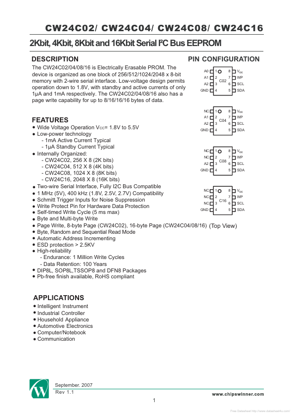
The CW24C02/04/08/16 is Electrically Erasable PROM.
The device is organized as one block of 256/512/1024/2048 x 8-bit memory with 2-wire serial interface.
Low-voltage design permits operation down to 1.8V, with standby and active currents of only 1μA and 1mA respectively.
| Part number | CW24C02 |
|---|---|
| Manufacturer | ChipsWinner |
| File Size | 275.91 KB |
| Description | (CW24C02 - CW24C16) I2C Bus EEPROM |
| Datasheet |
CW24C02 Datasheet
|
|
|
|
| Part Number | Description | Manufacturer |
|---|---|---|
| CW201212 | High Q Chip Inductors | Bourns |
| CW2013 | Low-Cost 1s Fuel Gauge | Cellwise |
| CW2015 | Low-Cost Fuel Gauge | Cellwise |
| CW2017 | Lithium-ion Fuel Gauge | Cellwise |
| CW20P | CW20P-Type CW Tunable/ Wavelength-Stabilized Laser Module | Agere Systems |
| Part Number | Description |
|---|---|
| CW24C04 | (CW24C02 - CW24C16) I2C Bus EEPROM |
| CW24C08 | (CW24C02 - CW24C16) I2C Bus EEPROM |
| CW24C128 | 128Kbit and 256Kbit Serial I2C Bus EEPROM |
| CW24C16 | (CW24C02 - CW24C16) I2C Bus EEPROM |
| CW24C256 | 128Kbit and 256Kbit Serial I2C Bus EEPROM |
The following content is an automatically extracted verbatim text from the original manufacturer datasheet and is provided for reference purposes only.