Datasheet Summary
CED603AL/CEU603AL
N-Channel Enhancement Mode Field Effect Transistor Features
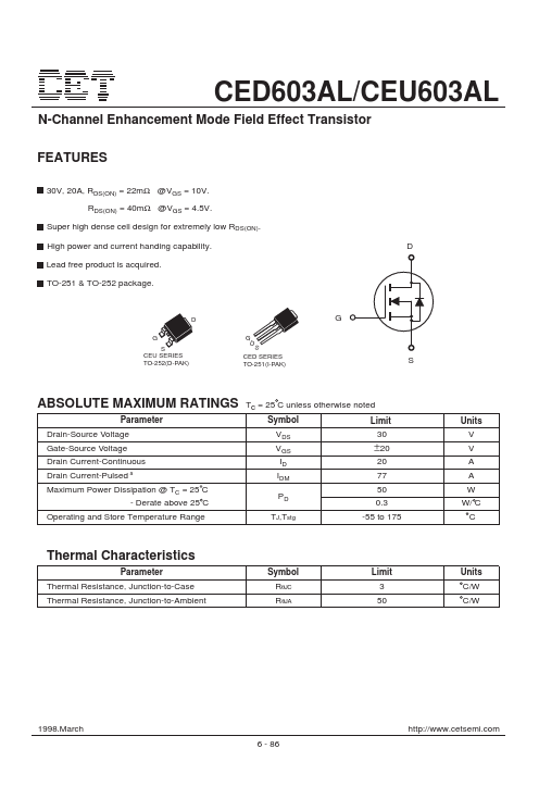
30V, 20A, RDS(ON) = 22mΩ @VGS = 10V. RDS(ON) = 40mΩ @VGS = 4.5V. Super high dense cell design for extremely low RDS(ON). High power and current handing capability. Lead free product is acquired. TO-251 & TO-252 package. D
D G S CEU SERIES TO-252(D-PAK)
S CED SERIES...