CEU40N10 Overview
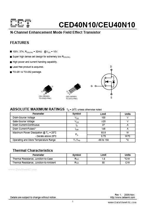
N-Channel Enhancement Mode Field Effect Transistor.
CEU40N10 datasheet by Chino-Excel Technology.
This datasheet includes multiple variants, all published together in a single manufacturer document.
| Part number | CEU40N10 |
|---|---|
| Datasheet | CEU40N10 CEU40N10_Chino Datasheet (PDF) |
| File Size | 442.76 KB |
| Manufacturer | Chino-Excel Technology |
| Description | N-Channel MOSFET |
|
|
N-Channel Enhancement Mode Field Effect Transistor.
View all Chino-Excel Technology datasheets
| Part Number | Description |
|---|---|
| CEU4201 | P-Channel MOSFET |
| CEU01N65 | N-Channel MOSFET |
| CEU01N65A | N-Channel MOSFET |
| CEU01N6G | N-Channel MOSFET |
| CEU01N7 | N-Channel MOSFET |
| CEU02N6G | N-Channel MOSFET |
| CEU02N7G | N-Channel MOSFET |
| CEU04N7G | N-Channel MOSFET |
| CEU05P03 | P-Channel MOSFET |
| CEU10P10 | P-Channel MOSFET |