CEU3060 Overview
Key Features
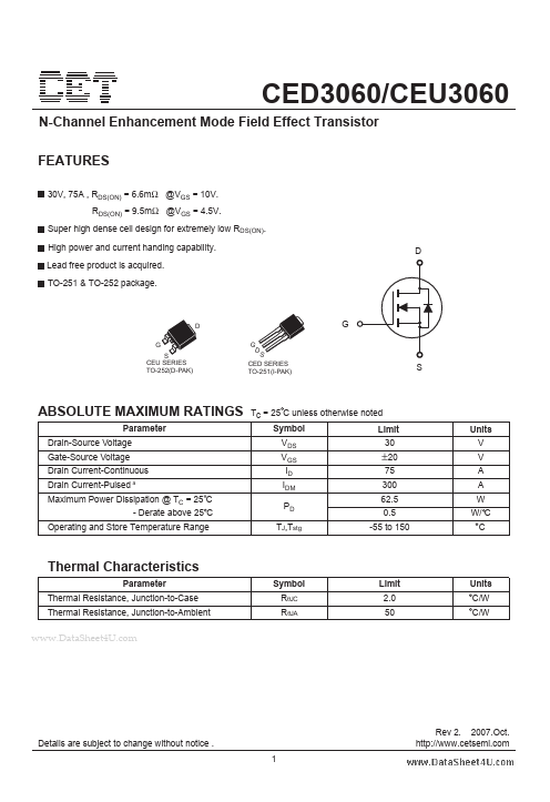
- 30V, 75A , RDS(ON) = 6.6mΩ @VGS = 10V
- RDS(ON) = 9.5mΩ @VGS = 4.5V
- Super high dense cell design for extremely low RDS(ON)
- High power and current handing capability
- Lead free product is acquired
| Part | CEU3060 |
|---|---|
| Description | N-Channel MOSFET |
| Category | MOSFET |
| Manufacturer | Chino-Excel Technology |
| Size | 417.41 KB |
| Seller | Inventory | Price Breaks | Buy |
|---|---|---|---|
| UnikeyIC | 400000 | 100+ : 0.2393 USD 200+ : 0.2353 USD 300+ : 0.2293 USD |
View Offer |
| Unikeyic (ICkey) | 400000 | 100+ : 0.2393 USD 200+ : 0.2353 USD 300+ : 0.2293 USD |
View Offer |
| Part Number | Manufacturer | Description |
|---|---|---|
| AP9563GH | Advanced Power Electronics Corp | P-CHANNEL ENHANCEMENT MODE POWER MOSFET |
| A2SHB | HAOHAI | N-Channel MOSFET |
| FCPF360N65S3R0L | onsemi | N-Channel MOSFET |