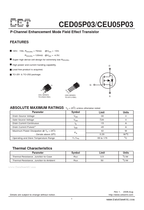
• Part: CEU05P03
  • Description: P-Channel MOSFET
  • Category: MOSFET
  • Manufacturer: Chino-Excel Technology
  • Size: 121.33 KB
Download CEU05P03 Datasheet PDF
Chino-Excel Technology
CEU05P03
CEU05P03 is P-Channel MOSFET manufactured by Chino-Excel Technology.
- Part of the CEU05P03_Chino comparator family.
FEATURES -30V, -15A, RDS(ON) = 70mΩ @VGS = -10V. RDS(ON) = 120mΩ @VGS = -4.5V. Super high dense cell design for extremely low RDS(ON). High power and current handing capability. Lead free product is acquired. TO-251 & TO-252 package. D D G S CEU SERIES TO-252(D-PAK) S CED SERIES TO-251(I-PAK) ABSOLUTE MAXIMUM RATINGS Parameter Drain-Source Voltage Gate-Source Voltage Drain Current-Continuous Drain Current-Pulsed a Tc = 25 C unless otherwise noted Symbol Limit VDS VGS ID IDM PD TJ,Tstg -30 Units V V A A W W/ C C ±20 -15 -45 42 0.29 -55 to 175 Maximum Power Dissipation @ TC = 25 C - Derate above 25 C Operating and Store Temperature Range Thermal Characteristics Parameter Thermal Resistance, Junction-to-Case Thermal Resistance, Junction-to-Ambient Symbol RθJC RθJA Limit 3.5 50 Units C/W C/W .. Details are subject to change without notice . 1 Rev 1. 2006.Aug http://.cetsemi. CED05P03/CEU05P03 Electrical Characteristics Parameter Off Characteristics Drain-Source Breakdown Voltage Zero Gate Voltage Drain Current Gate Body Leakage Current, Forward Gate Body Leakage Current, Reverse On Characteristics b Gate Threshold Voltage Static Drain-Source On-Resistance Forward Transconductance Dynamic Characteristics Input Capacitance Output Capacitance Reverse Transfer Capacitance Switching Characteristics c Turn-On Delay Time Turn-On Rise Time Turn-Off Delay Time Turn-Off Fall Time Total Gate Charge Gate-Source Charge Gate-Drain Charge Drain-Source Diode Forward Current Drain-Source Diode Forward Voltage b td(on) tr td(off) tf Qg Qgs Qgd IS VSD VGS = 0V, IS = -7.5A VDS = -15V, ID = -7.5A, VGS = -10V VDD = -15V, ID = -1A, VGS = -10V, RGEN = 6Ω 8 11 23 14 22.5 2 6 -15 -1.3 15 20 40 25 29 ns ns ns ns n C n C n C A V c Tc = 25 C unless otherwise noted Symbol BVDSS IDSS IGSSF IGSSR VGS(th) RDS(on) g FS Ciss Coss Crss Test Condition VGS = 0V, ID = -250µA VDS = -30V, VGS = 0V VGS = 20V, VDS = 0V VGS = -20V, VDS = 0V VGS = VDS, ID = -250µA VGS = -10V, ID = -7.5A VGS =...